| CATEGORII DOCUMENTE |
| Bulgara | Ceha slovaca | Croata | Engleza | Estona | Finlandeza | Franceza |
| Germana | Italiana | Letona | Lituaniana | Maghiara | Olandeza | Poloneza |
| Sarba | Slovena | Spaniola | Suedeza | Turca | Ucraineana |
Model 2800
Kilowatt Mosfet Audio Amplifier
Table Of Contents
Audio Amplifier Section
|
Introduction Amplifier Overview Amplifier Features Amplifier Topology Getting Started |
Protection Section
|
Amplifier & Speaker Protection Overview Amplifier Protection Controller Amplifier External Load Detector Amplifier Rail Detector Amplifier DC Offset Detector Amplifier Short Circuit Detector Amplifier Temperature Detector Input |
Construction Notes
|
Component Reference Designators Component Assembly Order Component Orientation Component Installation Preliminary Test Finally Assembly Final Test Matching Mosfet Transistors Audio Amplifier Section Parts List Protection Section Parts List Schematics |
Introduction
The goals for the DIY amplifier project was to design a low noise class ab mosfet amplifier that is able to deliver
high power into an 8 ohm load, be 2 ohm stable and drive 1 ohm speakers playing music not continuous test tones.
The amplifier will use discrete circuits with no signal processing and will include a differential input stage, large bank of output stage transistors and have the ability to bridge two channels to create a single even more powerful monoblock amplifier.
Instead of designing an amplifier from scratch, one DIY amplifier design chosen that met the requirements has
already been designed and published by Anthony E. Holton. He designed many amplifiers and the AV800 design
was chosen for this project. You can find his designs on his website at the url at the bottom of this page. The
AV800 amplifier is rated for 800 watts continuous driving a 4 ohm load. He also designed a 1000 watts version of this design by increasing the rail voltage and increasing the output stage transistor bank. Both these versions are
able to drive 2 ohm loads short term providing anywhere from 1200 watts to 1600 watts.
This document describes the Model 2800 Kilowatt Mosfet Audio Amplifier circuit board which is a single channel
AV800 1KW design with extra features and modifications. The output power of these amplifiers is determined by
the power supply rail voltage and output stage redundancy. Using rail voltages between 95 volts and 100 volts
can achieve approximately 1600 watts into 2 ohms short term, but overall nominal rail voltage of 90 to 95 volts will
work nice to create a cushion of safe operating area for the amplifier with a small penalty to output power.
Anthony E. Holton wrote the original documentation to describe the AV800 amplifier. Some of his documentation has been included here, but it may have been altered to reflect the Model 2800 printed circuit board and schematic. You can refer to the AV800 construction manual for reference but the component reference designators on his documentation will not match the Model 2800 printed circuit board. Use the schematic in this document.
Anthony E. Holtons website
https://www.aussieamplifiers.com/
Amplifier Overview
AV800 Amplifier
The AV800 is rated for 800 watts and has been tested by Anthony Holton to output continuous power of 450 watts
into 8 ohms, 820 watts into 4 ohms, and short term power of 1200 watts into 2 ohms using 90 volt rails. Its a four
stage amplifier consisting of a differential input stage, voltage amplification stage, bias/buffer stage, and output stage. The output stage consists of 7 output stage transistors per voltage rail (14 transistors per channel).
AV800 - 1KW Amplifier
The AV800 - 1KW is the same amplifier as the AV800 except it uses more output stage transistors and higher
voltage rails to achieve a power rating of 1000 watts. Anthony Holton has tested the continuous output power of
550 watts into 8 ohms, 1050 watts into 4 ohms, and short term power of 1600 watts into 2 ohms using 96 volt rails
loaded The output stage consists of 10 output stage transistors per voltage rail (20 transistors per channel).
Model 2800 Kilowatt Mosfet Audio Amplifier
Refer to the Amplifier Features section below for additional information. To summarize, the Model 2800 printed
circuit board includes a SINGLE CHANNEL AV800 1KW design plus the following;
More output stage transistors, up to 28 per channel.
More on-board power supply capacitance, typically 13,000uF 28,000uF depending on capacitors chosen.
More on-board VAS capacitance, typically 3,000uF 6,000uF depending on capacitors chosen.
Protection circuits including a programmable controller with soft start that drives a high current speaker relay.
PCB footprints allow the installation of high quality polypropylene capacitors.
On-board beryllium copper fuse holders (clips) that support 30 amperes for each rail.
Input signal terminal block (3 pin) for (+) input, (-) input and also has a center ground pin for esoteric needs.
Molex connectors power input (6 pin) and speaker output (2 pin). Extra parallel pins for redundancy.
Four layer printed circuit board layout with power and ground planes and power redundant tracks.
The Model 2800 printed circuit board is designed to allow up to 14 output stage transistors per voltage rail
(28 transistors per channel). This is 8 more output stage transistors than the AV800 1KW amplifier and it should
allow 2 ohm continuous operation and perhaps 1 ohm music if adequate heatsinking is provided. The output impedance of the buffer stage may need adjustment to drive the extra Hexfet transistors, its unknown at this time.
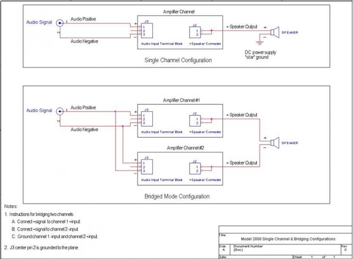
Single Channel Configuration
Refer to the Model 2800 - Single Channel and Bridging Configurations schematic for the wiring diagram. Single
channel configuration is the most common where one Model 2800 printed circuit is one amplification channel.
Connect the audio signal positive (+) to the positive (+) input on the terminal block.
Connect the audio signal negative (-) to the negative (-) input on the terminal block.
The terminal block center pin is grounded to the plane and may be used for esoteric needs such as shielding, etc.
The speaker output Molex connector connects to the (+) speaker terminal.
The (-) speaker terminal connects to the DC power supply star ground.
Bridged Mode Configuration
Refer to the Model 2800 - Single Channel and Bridging Configurations schematic for the wiring diagram.
Bridge Mode is when you use two amplifier channels connected together to form a single channel of greater power than a single channel, theoretically 4x more power, but typically 2x more power often referred to as a monoblock.
Connect the audio signal positive (+) to channel 1 positive (+) input and connect it to channel 2 negative (-) input.
Connect the audio signal negative (-) to channel 1 negative (-) input and connect it to channel 2 positive (+) input.
Connect the speaker across both positive outputs of both channels only. Do not connect the speaker the negative
or ground speaker terminals.
Channel 1 + speaker output connects to the + speaker terminal.
Channel 2 + speaker output connects to the speaker terminal.
Amplifier Features
AV800 Specifications
|
Specifications |
AV800 - 800 Watt |
AV800 - 1000 Watt |
|
8 Ohm Power Ratings |
450 W RMS continuous |
550 W RMS continuous |
|
4 Ohm Power Ratings |
820 W RMS continuous |
1050 W RMS continuous |
|
2 Ohm Power Ratings |
1200 W RMS short term |
1600 W RMS short term |
|
Frequency Response |
10HZ 100KHZ |
10HZ 100KHZ |
|
Distortion @ 1KHZ (100W into 8 Ohms) |
0.01% THD |
0.01% THD |
|
Damping Factor | ||
|
Voltage Rails |
+90V, -90V |
+110V, -110V (Loaded = +96V, -96V) |
|
Output Stage Transistors per Rail | ||
|
Power Supply Capacitance |
10,000 uF |
10,000 uF |
Model 2800 Minor Electrical Modifications
|
Modifications |
Model 2800 |
AV800 800W |
AV800 1KW |
|
Output Transistors |
14 per voltage rail 28 per channel |
7 per voltage rail 14 per channel |
10 per voltage rail 20 per channel |
|
On-Board Power Supply Capacitance |
9, 520 uF per voltage rail 19,040 uF per channel |
329 uF per voltage rail 658 uF per channel |
470 uF per voltage rail 940 uF per channel |
|
VAS Capacitance |
2,040 uF per voltage rail 4,080 uF per channel |
220 uF per voltage rail 440 uF per channel |
220 uF per voltage rail 440 uF per channel |
Model 2800 Protection Circuits
|
Circuit Name |
Description |
Author |
|
Protection Controller |
Main controller that receives input from the protection circuits. It also functions as an eight second turn-on delay to drive the speaker relay. |
DreadLordpk |
|
Rail Detector |
Monitors rail voltage imbalance. |
DreadLordpk |
|
External Load Detector |
Monitors the speaker terminals for abnormal resistive load during the initial power on sequence, then the circuit is disconnected when the speaker relay engages. This detector has user programmable load settings and its used to detect wiring errors or if an incorrect load was connected to the amplifier. |
DreadLordpk |
|
DC Offset Detector |
This is an ordinary common dc offset detector. |
Public Domain |
|
Output Short Circuit Detector |
This is an ordinary common output short circuit detector. |
Public Domain |
|
Clipping Detector |
This is the Rob Elliot clipping detector. https://sound.westhost.com/index.html |
Rob Elliot |
|
Rail Fuses |
The printed circuit board accommodates AGC solder mount fuse clips. Beryllium copper recommended over standard tin type fuse clips. | |
|
Temperature Detector Input |
This input accommodates a ground triggered temperature switch configuration. |
Model 2800 Printed Circuit Board Information
|
Item |
Description |
|
4 Layer Printed Circuit Board |
Top Layer 1 - Component side, power and ground tracks, alternative routing. Inner Layer 2 - Speaker output plane, protection circuit power supply plane. Inner Layer 3 - primary power & ground plane, ground barriers to steer ground currents. Bottom Layer 4 - Primary amplifier signal routing, power and ground tracks. |
|
Printed Circuit Board Properties |
1. Board size: 6.5W x 10.75L 2. Material: 125 mils thick epoxy-fiberglass, grade FR-4. 3. Finish: Gold-over-nickel 4. Soldermask both sides, LPI or equivalent, color = red 5. Top layer silkscreen using white non-conductive CAT-L-Link or equivalent. 6. 25 mils minimum separation between layers. |
|
Power & Ground Redundancy |
Top & bottom layer have extra power & ground tracks in parallel with layer 3 power & ground plane. |
|
On-Board Transistor Mounting |
There are three output stage transistor mounting schemes. Vertical, horizontal, and underneath the board. There are surface mount pads on the top and bottom of the board and two sets of holes for soldering. |
|
Power Supply Capacitors |
Supports up to 750 mil diameter capacitors using a 300 mil lead space. There are 14 capacitor footprints per voltage rail and also supports 3 capacitors for the VAS per rail. |
|
Molex Power & Speaker Connectors |
Designed for Molex Mini-Fit Sr. connectors. The speaker output uses a 2 pin connector and the power input uses a 6 pin connector. The contacts are rated for 50 amperes. The design uses two pins per function for reliability, i.e. both pins on the speaker output are shorted on the PCB. A similar setup for the power input is used. |
|
DPDT Speaker Relay |
Paralleled contacts for increased current capability and reliability. Relay N.O. contact ratings are; Resistive Load: 120/277 VAC 30 ampere per contact. 28 VDC 20 ampere per contact. |
|
Input Signal Terminal Block |
Supports a standard terminal block of 650 mil x 475 mil, 200 mil centers. |
|
Black Gate Capacitor |
Optional support for a single Black Gate 300uF 100V N series capacitor for the feedback loop. 18mm x 36mm |
|
Polypropylene Capacitor |
Large capacitor PCB footprints to allow the use of signal path polypropylene capacitors where applicable. |
|
Radial Source Resistors |
Supports radial source resistors with 200 mil lead space to save PCB real estate. |
|
Protection Circuit SMD |
The protection circuits are 100% surface mount devices to save PCB real estate. |
|
Signal Interface Connector |
This connector is used to provide inputs/outputs for interfacing such as controller status output, clipping detector output, external load detector output, temperature sensor input, muting input, interrupt input. |
Amplifier Topology
by Anthony E. Holton
Modified by DreadLordpk
The Error Amp Stage (Differential)
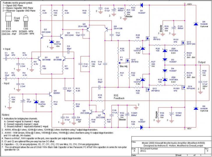
The first stage is what I call an asymmetrical balance input error amplifier. It is a design which allows only one single differential stage and yet has the ability to accept a balanced input source. An unbalanced source can be used if either the inverting or non-inverting input is tied to signal ground. Now I will explain how each device in the stage works together. Q1, Q2, R6, R7, R8, R9 form the main differential error amplifier which then has its collectors connected to a cascode load. Q3, Q4, R10 and ZD1 form the cascode stage which provides a constant 14.4 volts on the collectors of Q1, Q2. Q5, R11, R12, ZD2 and C6 form a constant current source which supplies 1.5 milliamps to the first differential stage. These modules form the first stage of the amplifier and basically set up how the whole amplifier is biased from front to back.
The Voltage Amplification Stage
This next stage provides most of the voltage amplification that the next stage needs to drive the output stage to full power. Q6, Q7, Q8, Q9, R16, R17, R18, R19, C10, C15, C16, C2901, C3401 for the second differential voltage amplification stage. Q6 and Q7 form what is known as a current mirror load for the second differential stage and basically force this stage to share the current supplied from R36, which is about 8 milliamps. The remaining components, namely the capacitors C11, C12 provide local frequency compensation for this stage.
The Bias and Buffer Stage
As the name suggest Q10, Q11, Q12, R27, R25, R26, R22, R20, R21, C14, ZD3, ZD4, form the bias and buffer stages. Its main purpose is to provide the mosfet gates with a stable and compensated supply voltage and buffer the voltage amp stage from the high gate source capacitance. Which would without this stage cause the frequency response and slew rate to be very poor indeed. The down side of this is the extra stage does introduce and extra dominant pole into the amplifiers feedback loop.
The Output Stage or Current Amplification Stage
Once again as the name suggest this stage converts the voltage developed in the VAS and provides all the amperes needed to drive 8 or 4 Ohm loads. 2 Ohm loads are possible for several minutes at a time. In fact, I have tested the 1KW amplifier to over 1600 watts RMS into 2 Ohms. But this would not be recommended as a long-term load at all. As it does exceed the SOA figures of the output stage.
Note: Model 2800 with 28 output transistors and robust heatsinking should be able to drive a 2 Ohm load continuous tone testing. It may even drive a 1 Ohm load playing music, not continuous test tones.
Power Supply Requirements
The power supply components for this amplifier are as
follows and are expressed for one channel or one power module only. 1 x toroidal transformer
with a core rating of 1KVA. Primary windings are made to suit your local mains supply, e.g.: for
The secondary windings are as follows.
2 x 65 volts AC at full load.
One 400 volt 35 ampere bridge rectifier.
2 x 4.7K 5 watt ceramic resistors.
Minimum filter capacitor requirements would be 2 x 10,000 uF 100 volt electrolytic
Ideal capacity would be 40,000 uF per voltage rail.
For stereo or dual mono operation the following power supply will be required.
1 x 2KVA toroidal transformer with a core rating of 2KVA.
2 x 400 volt 35 ampere bridge rectifier.
4 x 10,000 uF 100 volt electrolytic capacitors.
2 x 4.7K 5 watt ceramic resistors.
Getting Started
This section assumes you have read this whole document and you have completed the assembly of the amplifier
and tested all the circuits. There are a few things to configure before using the amplifier. There are some
programmable settings of the Protection Controller and the External Load Detector that need to be set.
Protection Controller Setup
Refer to the Amplifier Protection Controller section for reference. Use the DIP Switch labeled S1 on the printed
circuit board to configure the Controller. See Figure 1 for the location of the DIP switch.
1. Determine which protection circuits you want enabled and turn ON the appropriate DIP switches , S102 - S502.
If you want all the protection circuits enabled, simple turn ON all the switches S102 through S502.
2. Determine if you want the amplifier to operate in Latch Mode (switch ON) or Loop Mode (Switch OFF) and set
DIP switch S602. Latch mode requires the user to turn OFF the amplifier to reset faults,
In Loop Mode, the Protection Controller will restart when the faults clears and return to normal operation.
External Load Detector Setup
Refer to the Amplifier External Load Detector section for reference. Use DIP Switch labeled S2 on the printed circuit board to configure the External Load Detector. See Figure 1 for the location of the DIP switch.
1. Determine the resistance threshold that will cause the ELD to trigger a fault condition and set the appropriate
sequence of switches S104 S504.
2. For non-bridged mode operation, set the amplifier channel to Master mode by turning OFF the Master/Slave
switch S604. You can use the Slave Mode for non-bridged operation, the only minor drawback is the self check
stops functioning 2 seconds after the amplifier is powered on.
3. For bridged mode operation, you need to jumper two wires across both amplifier channels for communications
and set one channel for Master Mode and set the other channel for Slave mode. The Interface Connector
is used for this function. Refer to the Amplifier Protection Controller section for information on the Interface
Connector and see Figure 1 for additional reference of pin locations.
Interface Connector
Refer to the Amplifier Protection Controller section for reference. Determine if you require any additional connections to be wired to this interface connector such as the clipping LED, temperature sensor, muting and
bridged-mode wiring. The amplifier will still function if you choose to make no connections, these are extra
features that you access through this connector. See Figure 1 for additional reference of pin locations.
Amplifier & Speaker Protection Overview
Design Methodology
The design methodology chosen for amplifier and speaker protection is based on using a high current relay between the amplifiers output and the speaker using the normally open relay contacts. The relay must be turned on to connect the speaker to the amplifier. When a fault occurs, the relay will turn off and disconnect the speaker from the amplifier.
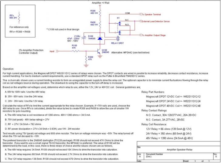
Speaker Relay
The common relay used in the home and car audio industry is the Potter & Brumfield 30A SPST relay (T9AS5D12 series). The relay chosen for this design is the Magnecraft 30A DPDT relay (W92S11D12 series). The DPDT relay contacts are connected in parallel for the benefits of 60A capability, contact redundancy for reliability and provide less relay contact resistance.
Speaker Relay Pros
Disconnect the speaker from the amplifier when a fault occurs to protect the speakers.
Speaker Relay Cons
Some audiophiles claim that relays may have a sonic signature typically due to poor electrical contact between the amplifier and the speaker. The relay chosen and the configuration used should alleviate the fear of using relays even for the most critical audiophiles.
The other concern with using a speaker relay is voltage may arc across the relay contacts causing contact failure. This occurs during a high voltage DC offset failure or similar failure of the amplifier. The design uses two diodes on the normally closed contacts to shunt any high voltage arcs to ground. Its not a 100% solution but it may prolong relay contact life. Worse case, if there is a severe amplifier failure and the relay is damaged in the process of saving your $10,000 speakers, the cost to replace the relay is $10, a better solution than replacing a speaker system.
Protection Detectors
There are five detectors, Rail Detector, External Load Detector, DC Offset Detector, Short Circuit Detector and an external input for temperature detection using a thermal switch or equivalent. Included is voltage rail fuse holders on the printed circuit board capable of 30A each.
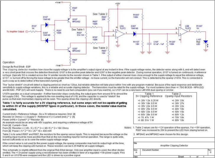
Clipping Detector
The Rob Elliot clipping detector is used in this design for visual indication when the amplifier is clipping the audio signal. It doesnt interact with the Protection Controller.
Rob Elliots website
https://sound.westhost.com/index.html
User Programmable Settings
There are two banks of DIP switches, one for the Protection Controller and one for the External Load Detector to select desired modes of operation.
Status LEDs
There are nine system status LEDs.
Interface Header
There is a 6 pin interface header used for input/output functions and ease of wiring.
Amplifier Protection Controller
Description
Its function is to determine when to turn on/off the speaker relay using data it receives from the detectors/inputs.
Protection Controller Functions
1. Provides an 8 second delay before turning on the speaker relay to protect the speaker from turn-on transients.
2. Receives pass/fail status from all the protection detectors.
3. Controls the speaker relay.
4. Two modes of
operation, Latch or
5. User can enable/disable each detector via a DIP switch bank.
Protection Controller Inputs
1. Rail Detector Input.
2. External Load Detector Input.
3. DC Offset Detector Input.
4. Short Circuit Detector Input.
5. Temperature Detector Input.
6. Muting Input (External).
7. Interrupt input (External).
Protection Controller Outputs
1. Controller Status Output.
2. Clipping Detector LED Output
3. External Load Detector Output (used for Bridged Mode Testing)
User Programmable Settings
The Protection Controller has a DIP switch bank (S1 on the circuit board) to enable/disable individuals Detectors.
S102 ON = enable the External Load Detector.
S202 ON = enable the Rail Detector.
S302 ON = enable the DC Offset Detector.
S402 ON = enable the Temperature Detector.
S502 ON = enable the Short Circuit Detector.
S602 ON = Latch Mode, OFF =
Latch mode requires the user to turn OFF the amplifier to reset
faults,
Protection Controller will restart when the faults clears and return to normal operation.
Status LEDs
There are nine status LEDs to help the user in determining any system faults. The LEDs are not latched, therefore if a fault clears the LED will turn off automatically.
1. Six Detector LEDs (Red), one for each Detector. When a Detector sends a fault signal, the LED will light up.
2. Status Output LED (Green). The LED with light up when the speaker relay is turned on.
3. Master/Slave LED (Blue). The LED with light up when placed in the Slave Mode. Used by ELD.
4. Interrupt LED (Yellow). The LED with light up when the amplifier channel is being interrupted. Used by ELD.
Interface Header
Use the interface header to wire any inputs or outputs as needed.
1. Status Output (ST). This is a ground output when armed.
2. Clipping LED Output (CD). This is a positive output that connects to the LED anode. Connect the cathode
to power supply ground.
3. External Load Detector (ED). This is a ground output when a fault is detected.
4. Temperature Switch Input (TD). Use a ground signal to indicate a fault.
5. Muting Input (MT). Use a ground signal to mute the speaker relay (turn it off).
6. Interrupt Input (INT). Use a ground signal to interrupt the External Load Detector.
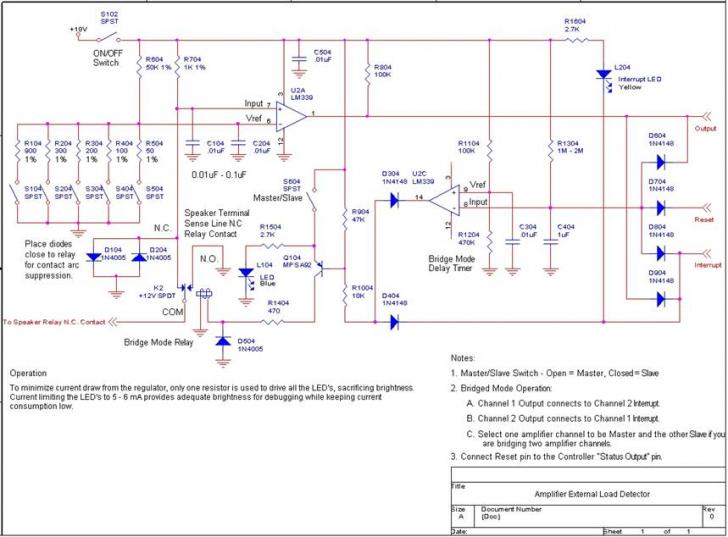
Amplifier External Load Detector
Description:
The External Load Detector (ELD) monitors the speaker terminal for an abnormal resistive load during the initial amplifier power on sequence to detect wiring errors, shorts, or incorrect speaker load. The ELD is NOT directly connected to the speaker terminal, it uses the speaker relay normally closed contacts to sense the load present only when the relay is turned off. When the speaker relay turns on, the ELD is disconnected from the speaker terminals. The user determines the triggering threshold by programming the DIP switch (S2 on the circuit board).
The ELD is a comparator that measures the resistive load on the amplifiers speaker terminals in reference to ground and compares this value to the threshold resistance value that the user programmed. If the load present at the speaker terminal is lower in resistance than the preset value, an error output will trigger. For bridge mode operation and additional measurement is made between both positive terminals of the two channels. Anytime the speaker relay is off, the ELD is measuring the load on the speaker terminal.
Speaker Relay COM contact = Amplifier Speaker Terminal
Speaker Relay N.O. contact = Amplifier Output
Speaker Relay N.C. contact = External Load Detector
Programmable Threshold Setting:
DIP switch bank (S2) on the circuit board is used to program the ELD, specifically switches S104 through S504. S604 is used for bridge mode operation to set the Master/Slave function of the ELD.
Referring to Table 1, determine the detection threshold that will create an error output. Example, if you want to the ELD to trigger when the load resistance is less than 1.5 ohms, you turn ON switches S204 and S404, the rest are turned OFF. If there is a resistive load present on the speaker terminal in reference to ground that is less than 1.5 ohms, the ELD will trigger.
Table 1 External Load Detector DIP Switch Settings
|
Threshold |
Equivalent Detector Ohms |
Switch S104 R104 = 900 Ohms |
Switch S204 R204 = 300 Ohms |
Switch S304 R304 = 200 Ohms |
Switch S404 R404 = 100 Ohms |
Switch S504 R504 = 50 Ohms |
|
0.5 Ohms |
25 Ohms |
ON |
ON |
ON |
ON |
ON |
|
0.8 Ohms |
40 Ohms |
OFF |
OFF |
ON |
OFF |
ON |
|
1.0 Ohms |
50 Ohms |
OFF |
OFF |
OFF |
OFF |
ON |
|
1.5 Ohms |
75 Ohms |
OFF |
ON |
OFF |
ON |
OFF |
|
2.0 Ohms |
100 Ohms |
OFF |
OFF |
OFF |
ON |
OFF |
|
2.4 Ohms |
120 Ohms |
OFF |
ON |
ON |
OFF |
OFF |
|
3.26 Ohms |
163 Ohms |
ON |
OFF |
ON |
OFF |
OFF |
|
4.0 Ohms |
200 Ohms |
OFF |
OFF |
ON |
OFF |
OFF |
|
4.5 Ohms |
225 Ohms |
ON |
ON |
OFF |
OFF |
OFF |
|
6.0 Ohms |
300 Ohms |
OFF |
ON |
OFF |
OFF |
OFF |
1. The comparator Vin resistor is 1K Ohms (R704) in series with the Rload (load across speaker terminals).
2. The comparator Vref resistor is 10K Ohms (R604) in series with the resistance values shown on Table 1.
3. The DIP switch resistors were scaled upwards in Ohms by a factor of 50 times to allow better precision, i.e., Threshold x 50 = Equivalent Detector Ohms.
Normal Operation (single amplifier channel):
1. To enable the ELD, S102 must be set to the ON position.
2. Set the Master/Slave switch to 'Master' on the amplifier channel.
3. Set the triggering threshold that you desire as shown in Table 1.
During the amplifier power on sequence, the ELD will immediately measure the resistance between the speaker terminal in reference to ground. If it measures less resistance than the programmed threshold, the ELD will trigger an output ground signal.
Bridged Mode Operation (two amplifier channels connected to form a more powerful single channel amplifier):
In order for the ELD to function correctly in this configuration, you need to jumper two wires across both channels for communications. These two wires do not need to be removed if you are in Normal Operation. Refer to the section below called Bridge Mode Wiring for details.
1. Bridge Mode Wiring for inter-channel communications must be enabled.
2. To enable the ELD, S102 must be set to the ON position.
3. Set the Master/Slave switch to 'Master' on one amplifier channel, set the other amplifier channel to Slave.
4. Set the triggering threshold that you desire as shown in Table 1.
Due to the loading effects of both amplifier channels, the ELD will only trigger when the measured load across both speaker terminals is of the programmed threshold value. Example, if you program the ELD for 1 ohm, in bridged mode only, if it measures less than 0.5 ohms between both speaker terminals, it will trigger. For measurements from speaker terminal to ground, it will function the same as Normal Operation, it will trigger if it measures 1 ohm in reference to ground.
There are two types of Bridged Mode tests.
1. Self Test The speaker terminal to ground is measured. This test is the same as Normal Operation.
2. Bridged Test If Self Test passes, the Bridge Mode testing will occur ~2 seconds after Self Test. The load across both speaker terminals (positive terminals of both channels) is measured. To measure the load across two floating terminals, the Slave channel will enable the Bridge Mode circuit which forces a low current ground signal to its positive speaker terminal to allow the Master channel to measure the load in reference to the ground present on the positive speaker terminal of the Slave channel.
Bridge Mode Sequence of Events;
Note: If Self Test fails, the master channel will interrupt the Slave channel and force the Bridge Mode relay on the Slave channel to turn on. This is a dont care situation because Self Test fails.
Bridged Mode Wiring:
1. Jumper a wire from channel #1 External Load Detector Output to channel #2 Interrupt Input.
2. Jumper a wire from channel #2 External Load Detector Output to channel #1 Interrupt Input.
3. One channel must to be set for 'Master' mode and the other channel must to be set for 'Slave' mode.
Notes:
1. These two jumper wires allow interrupt communications between both channels.
2. The Master channel will measure the load across both speaker terminals and its terminal to ground.
External Load Detector Control Pins:
1. Reset Turns off the Bridge Mode circuit including the Bridge Mode relay.
2. Interrupt - Force the Bridged Mode relay to turn on immediately or force it to stay on and reset the delay circuit.
If the Slave channel Self Test fails, it will not enter the Bridged Mode test. If Master channel detects a fault across both speaker terminals, the Master channel will send an interrupt signal to the Slave channel controller and it will also be connected to the Interrupt input of the delay/relay driver circuit to force the relay to stay turned on and to reset the delay. When the fault across the speaker terminal is removed (if the amplifier has not been turned off), then these sequence of events will occur;
1. The relay will turn off immediately.
2. The Slave channel will redo the self test.
3. If self test passed 2 seconds later, the delay circuit enables the relay and the Master channel repeats the test across both speaker terminals.
Amplifier Rail Detector
Description
The Rail Detector monitors the power supply rail voltages and triggers a fault when there is an imbalance between both voltages. The voltage differential threshold is programmable via two zener diodes. The default threshold is 10V +/- 2V.
The Rail Detector will detect these type of failures and trigger a fault condition;
1. One of two rail fuses blows. The Rail Detector may trigger when both fuses blow.
2. If one transformer fails in a dual transformer power supply design.
3. If the transformer is unbalanced or not loaded equally.
Turn Off Muting Operation
Turn off muting is a bonus feature that may function depending on your amplifier power supply design. When the amplifier is turned off and the power supply discharges quickly, the Rail Detector may detect the rapid discharge and trigger a fault condition that turns off the speaker relay which is a desirable feature to prevent turn-off transients reaching the speakers. Another method to achieve turn off muting is to create a condition that causes one power supply rail to discharge faster then the other rail. The Rail Detector will detect the voltage differential when exceeding the threshold and trigger a fault condition.
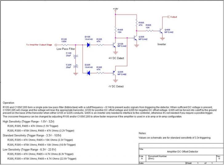
Amplifier DC Offset Detector
Description
The DC Offset Detector is a classic design used in the audio industry. It monitors the output stage and when sufficient DC voltage is present, it will trigger a fault condition. The sensitivity is programmable via three resistors with detection as low as 1.5V of DC offset.
Amplifier Short Circuit Detector
Description
The Short Circuit Detector is a classic design used in the audio industry, but implemented slightly different than conventional means. Normally an output series resistor is added between the amplifiers output stage and speaker and the voltage across the resistors is senses for over-current conditions. Adding this series resistor was rejected for sonic reasons. An alternative solution was to tap the sense line across on of the output transistors source resistor. In theory, all transistors should be sharing current equally and if an overload condition occurs, excess current with also flow thought the source resistor and trigger a fault condition. The sensitivity is programmable via a single resistor.
Amplifier Temperature Detector Input
Description
Temperature Detectors are not integrated into the design, but an input is provided to connect whatever temperature detection methods you prefer. A simple thermal switch (or switches) can be mounted on the heatsink and connect the switches to the temperature detector input wire on the 6 pin Interface Connector.
Component Reference Designators
The industry standard for component reference designator prefix is typically R for resistor, C for capacitor, D for diode, Q for transistor, J for connectors, etc. followed by a number (suffix) to identify the specific component. Example, R1, R2, R3, etc.
The reference designator scheme used is this design is different. The prefix is the same, but the suffix is different to identify which components below to a particular circuit. Example, the suffix 02 represents the Protection Controller. Any component with suffix 02 belongs to this circuit. The audio amplifier section use the industry standard method except for the output stage transistors and power supply capacitors See Table 2 for the list.
Table 2 Model 2800 Reference Designators
|
Circuit Name |
Reference Designator Suffix |
|
Audio Amplifier Section |
Industry Standard Suffix, i.e., R1, R2, R3, etc. The output stage transistors and power supply capacitors use 01 suffix, i.e., Q101, Q201, Q301, Q401, C101, C201, C301, C401, etc. |
|
Protection Controller |
02 suffix, i.e., R102, R202, R302, etc. |
|
Rail Detector |
03 suffix, i.e., R103, R203, R303, etc. |
|
External Load Detector |
04 suffix, i.e., R104, R204, R304, etc. |
|
DC Offset Detector |
05 suffix, i.e., R105, R205, R305, etc. |
|
Output Short Circuit Detector |
06 suffix, i.e., R106, R206, R306, etc. |
|
Clipping Detector |
07 suffix, i.e., R107, R207, R307, etc. |
|
Speaker Relay |
08 suffix, i.e., R108, R208, R308, etc. |
|
Protection Power Supply |
09 suffix, i.e., R109, R209, R309, etc. |
Component Assembly Order
The recommended component assembly order is shown in Table 3. Install and test each section one at a time for ease of debugging problems. Refer to the parts list and schematics at the bottom of this document. Figure 1 below shows the component placement map for the protection circuits located on the right side of the printed circuit board, the SMD components. For a more detailed explanation, see the installation guide below.
Table 3 Recommended Assembly Order
|
Component |
Comments |
|
Fuse 1 |
This is the positive power supply voltage rail fuse. Insert a fuse on both clips and solder the clips their location. |
|
Fuse 2 |
This is the negative power supply voltage rail fuse. Insert a fuse on both clips and solder the clips their location. |
|
K1 Speaker Relay |
This is the large speaker relay in the center of the printed circuit board. |
|
J1 Molex Connector |
This is the power supply input, +V, -V, and ground. Solder the 6 pin Molex connector in this location. |
|
J2 Molex connector |
This is the speaker output connector. Solder the 2 pin Molex connector in this location. |
|
Protection Power Supply |
The power supply is approximately +18v. |
|
Speaker Relay Driver |
Figure 1 - GRAY area. |
|
Protection Controller |
Figure 1 - RED area. |
|
Status LEDs |
Figure 1 - TEAL area. |
|
Short Circuit Detector |
Figure 1 - CYAN area. Q106 & R106 are the sensing components located next to Q1401 on the upper right location of the pcb. |
|
External Load Detector |
Figure 1 Blue area. |
|
Rail Detector |
Figure 1 GREEN area. |
|
DC Offset Detector |
Figure 1 - Light PINK area. |
|
Clipping Detector |
Figure 1 - YELLOW area. |
|
Interface Connector |
Figure 1 - PINK area. |
|
Audio Amplifier Section |
Left side of the printed circuit board. |
Component Orientation
Resistor Installation Orientation
Resistors have no polarity and can be installed in any orientation.
Capacitor Installation Orientation
The SMD capacitors are small in value and have no polarity and can be installed in any orientation. The larger capacitors do have polarity indicated on the schematic and labeled with a + sign on the printed circuit board. For example, if you look at figure 1 you will see capacitor C105 and C106 which has a plus sign (+) next to them indicating the installation orientation.
Diode Installation Orientation
All diodes including zener diodes have polarity and must be installed in the correct orientation. Zoom in on Figure 1 and you will see the printed circuit board silkscreen diode orientation. The diode prefix is labeled D and the symbol has two beveled edges to represent the diode cathode. You must place the diodes in the correct orientation for proper function.
Transistor Installation Orientation
All transistors have three leads and must be installed in the correct orientation. Bipolar transistor leads are base, emitter, collector. Mosfet transistor leads are gate, drain, source. For SMD transistors, the installation is easy because there is only one way the transistor will line up with the SMD component pads. For non-SMD transistors, the silkscreen will indicate B, C, E for the larger bipolar transistors. The output stage transistors are just labeled G for gate. The small signal transistors in the T0-92 package have not markings, but you can look at the silkscreen picture for correct match.
Component Installation
Reference the parts list, schematics, and Figure 1 for component values and installation locations. Its easier to install the surface mount devices (SMD) first then install the larger components. You will need a fine tipped soldering iron, fine awg solder, liquid flux and tweezers to hold the device or any other method you prefer. One technique to solder SMD devices is to place a tiny drop of flux on the SMD pad, apply a little solder to the pad using the soldering iron to coat the pad with a thin layer of solder. Place the SMD component on top of the pre-tinned pads and hold the device with the tweezers and heat up the intersections where the component meets the pad causing the soldering iron to reflow the solder.
Fuse Clip Installation (Fuse 1, Fuse 2)
The fuse clips are beryllium copper rated for 30 amperes. To get the best electrical connection install the fuse clips on the fuse and position the clips for best alignment. Install the fuse/clip assembly on the printed circuit board. Use a high wattage solder iron.
Speaker Relay Installation (K1)
This is the large speaker relay located in the center of the board. Its a DPDT relay with parallel contacts for high current capability and contact redundancy for improved reliability. Use a high wattage solder iron.
Molex Connector Installation (J1)
This is a 6 pin connector used for the power supply input, + voltage rail, - voltage rail, and ground. Solder the
6 pin Molex connector in this location. The two center pins are ground, the two top pins are positive rail, the
bottom two pins are the negative rail. The two pin parallel design allows a higher current capability up to 100
amperes and also provides contact redundancy to improve reliability. You can solder two wires in parallel on the
Molex receptacle, one set for the positive voltage rail, one set for the negative voltage rail, and one set for ground.
If you chose not to use the Molex connector, you can insert and solder a large diameter wire in the largest hole provided on the printed circuit board. Use a high wattage solder iron.
Molex Connector Installation (J2)
This is a 2 pin connector used for the speaker output connector. Both pins are shorted together on the printed circuit board. The two pin parallel design allows a higher current capability up to 100 amperes and also provides contact redundancy to improve reliability. If you chose not to use the Molex connector, you can insert and solder a large diameter wire in the largest hole provided on the printed circuit board. Use a high wattage solder iron.
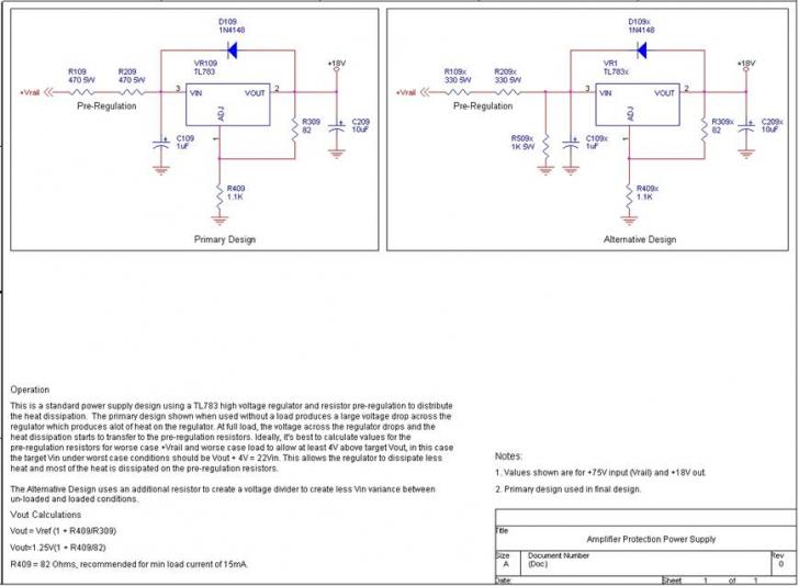
Protection Circuit Power Supply Installation
Install the protection circuit power supply. Temporarily mount a TO-220 heatsink or equivalent to the voltage regulator for testing purposes, then later you can remove the heatsink and mount the voltage regulator to the main heatsink used by the output stage transistors. Plug in the Molex connector and turn on the power supply. The voltage regulator should output approximately +18 volts +/- 1 volt.
Speaker Relay Driver Installation
Install resistors R108, R208, R308, R408
Install transistor - Q108
Note: R308 and R408 are 1W resistors.
Protection Controller Installation
Install integrated circuit U1
Install resistors - R102, R202, R302, R402, R502, R602, R702, R802, R902, R1002, R1102, R1202
Install capacitors - C102, C202, C302, C402, C502
Install diodes - D102, D202, D302, D402, D502, D602, D702, D802, D902
Install transistor - Q102, Q103
Install 6 pin DIP Switch S1
Install Red LEDs - L102, L202, L302, L402, L502
Install Yellow LED - L602
Install Green LED - L702
Short Circuit Detector Installation
Install resistors - R106, R206, R306, R406, R506, R606
Install capacitors - C106
Install diodes - D106, D206
Install transistor - Q106
External Load Detector Installation
Install integrated circuit U2
Install resistors - R104, R204, R304, R404, R504, R604, R704, R804, R904, R1004, R1104, R1204, R1304, R1404, R1504
Install capacitors - C104, C204, C304, C404, C504
Install diodes - D104, D204, D304, D404, D504, D604, D704, D804, D904
Install 6 pin DIP Switch S2
Install relay
Install Blue LED L104
Install Yellow LED L204
Note: R104 R704 are 1% tolerance.
Rail Detector
Install resistors - R103, R203, R303, R403, R503, R603, R703, R803, R903
Install capacitors - C103, C203, C303, C403, C503
Install diodes - D103, D203, D303, D403, D503
Install transistor - Q103, Q203, Q303, Q403
DC Offset Detector
Install resistors - R105, R205, R305, R405, R505, R605
Install diodes - D105, D205
Install transistor - Q105, Q205, Q305, Q405
Install capacitors - C105, C205
Clipping Detector
Install integrated circuit U3
Install resistors - R107, R207, R307, R407, R507, R607, R707, R807, R907, R1007, R1107, R1207, R1307
Install capacitors - C107
Install diodes - D107, D207, D307
Install transistor - Q107, Q207
Note: Clipping LED L107 is mounted on the chassis and use the interface connector for wiring.
Interface Connector
Install a standard 6 pin Molex header, 100 mil centers.
Figure 1 Protection Circuit Component Map
Audio Amplifier Section
Install all the components except for the output stage transistors which will be install last after testing.
|
Component |
Reference Designator |
Comments |
|
Watt Resistors |
R1, R2, R3, R4, R5, R6, R7, R8, R9, R12, R13, R14, R15, R16, R17, R19, R20, R21, R22, R23, R24, R25, R26, R28, R29, R101 through R2801 | |
|
1 Watt Resistors |
R10, R11, R18, R27, R30, R31, R32, R33, R34 | |
|
Potentiometer |
P1 | |
|
Diodes |
D1, D2, D3, D4, D5, D6, ZD1, ZD2, ZD3, ZD4, ZD5, ZD6 |
Note orientation on pcb. |
|
Transistors |
Q1, Q2, Q3, Q4, Q5, Q6, Q7, Q8, Q9, Q10, Q11, Q12 |
Note orientation on pcb. |
|
3 Watt resistors |
RS01 through RS28 |
Minimum 3 watt. Radial mount. |
|
Capacitors |
C1, C2 (optional) - Some people prefer no input signal capacitors if the preamp has low DC offset. Install two jumper wires on the C1 & C2 locations if the capacitors are not used so the input signal passes through. |
Electrolytic capacitor is only viable solution due to space restrictions on the pcb. |
|
Capacitors |
C5, C7, C11, C12, C13 |
Silver mica capacitor preferred. |
|
Capacitors |
C3, C4, C8, C10, C14 |
Polypropylene capacitor preferred. |
|
Capacitors |
C6 |
Electrolytic capacitor, not polarity. |
|
Capacitors |
C15, C16 |
Polypropylene or any film type capacitor preferred. |
|
Capacitors |
C17 |
250 Vac X2 rated capacitor. |
|
Feedback Capacitor |
Pick one installation option. A. Install a 220uF non-polarized in location C9. B. Install two 470uF polarized in location C9A and C9B |
If C9A & C9B is installed, jumper a wire across the extra C9A & C9B pads. |
|
Power Supply Capacitors |
C101 through C3401 |
Note polarity on pcb. |
|
Input Signal Terminal Block |
J3 | |
|
Output Stage Transistors |
Q101 through Q2801 |
Install these last after testing. |
Note: Transistor Q10 is the Vbe multiplier or bias compensation device. It needs to be mounted on the same
heatsink that the output stage transistors are mounted to for thermal tracking.
Preliminary Test
The preliminary test will determine if the amplifier is functioning properly. The amplifier section of the printed circuit board should have all the components installed except the output stage transistors Q101 through Q2801.
To test the amplifier connect a 10 ohm watt resistor from the output of the amplifier to one side of the 330 ohm
1 watt resistor found at R27. This will connect the feedback resistor R15 to the output of the buffer stage and
bypass the output stage. Turn on the main power supply (+90v/-90v) and measure the voltage across these
resistors to verify that the amplifier is ok. If the amplifier passed these checks, power down the amplifier and remove the 10 ohm resistor.
R8 ~ 1.6 volts
R9 ~ 1.6 volts
R19 ~ 1.0 volts
R16 ~ 500mV
R17 ~ 500mV
Offset voltage at R15 should be close to 0 volts, but can be as high as 100mV.
Final Assembly
Transistor Matching
The output stage transistors need to be matched to ensure current sharing of the transistor bank. The N-channel
IRFP240 transistor bank should have similar electrical characteristics to each other and the P-channel IRP9240
transistor bank should have similar electrical characteristics to each other. You dont need to match N-channel
characteristics to P-channel characteristics. Refer to the section on Matching Mosfet Transistors.
Transistor Thermal Pads
The output stage transistors (IRFP240 & IRFP9240), the buffer stage transistors (IRF610 & IRF9610), and the protection circuit voltage regulator (TL783) are mounted on the same heatsink (or metal interface block). Insert a gray thermal pad (or equivalent) between the transistor and the heatsink. The gray thermal pads are designed for
electrical isolation and heat transfer, better than mica insulators in most cases. Refer to the manufacturers recommendation on whether or not you need thermal compound. If you use mica insulators, you need to apply
the white thermal compound to both sides of the insulator to transfer the heat from the transistor to the heatsink.
Transistor Clamping
There are two common methods to secure the transistor to the heatsink. You can use a thick metal bar that
spans the length of the transistor bank to clamp all the transistors firmly in place or you can individually screw
each TO247 package to the heatsink. If you use screws to secure the TO220 package make sure the screw doesnt touch the metal tab on the package otherwise the tab will short the heatsink. The metal tab on the
IRFP240, IRFP9240, IRF610, IRF9610 transistors are connected to the drain pin (middle pin). The metal tab on
the TL783 voltage regulator is connected to the output pin (middle pin). After the transistors and voltage regulator
have been clamped, use an ohm meter to verify that there is no electrical connection between the transistor
pin (that connects to the tab) and the heatsink.
Transistor to Heatsink Mounting Method 1
See Figure 2. The printed circuit board will mount on top of the heatsink using 1/4 standoffs minimum to provide ample clearance to avoid the bottom soldered leads from shorting to the heatsink. The transistor leads lay flat and are soldered on top of the printed circuit board pads. Use an aluminum interface block to couple the transistor to the heatsink.
Transistor to Heatsink Mounting Method 2
See Figure 3. The printed circuit board will mount on top of the heatsink using 1/4 standoffs minimum to provide ample clearance to avoid the bottom soldered leads from shorting to the heatsink. The transistor will lay flat on the heatsink underneath the printed circuit board. The transistor leads are bent 90 degrees and inserted through the holes on the printed circuit board from the bottom.
Note: There two sets of holes for the transistor. You can place the transistor further underneath the board by using the second set of holes.
Transistor to Heatsink Mounting Method 3
Note: The printed circuit board will mount on top of a mounting plate or chassis using 1/4 standoffs minimum to
provide ample clearance to avoid the bottom soldered leads from shorting to the heatsink. The transistor will mount vertical using the printed circuit board holes closest to the edge of the board. The transistor will be attached to the vertical heatsink.
Figure 2 Transistor to Heatsink Mounting Method 1
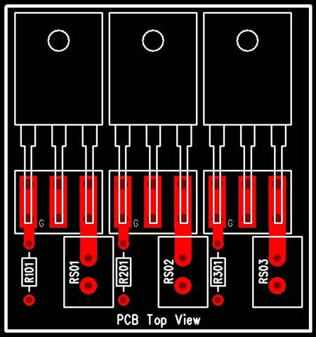

Figure 3 Transistor to Heatsink Mounting Method 2

Figure 4 Transistor to Heatsink Mounting Method 3

Final Test
Preliminary Checks
1. The drain pin on each output stage transistors are not shorted to the heatsink or block used for mounting.
2. The power supply wiring is the correct polarity.
3. The multi-turn potentiometer P1 has been turned back to 0 ohms so that a measurement of approximately
4.7K ohms is measured across the gate and drain pins of Q10.
4. Insert an 8 ampere fuse in each fuse holder on the printed circuit board, labeled FUSE 1 and FUSE 2.
5. Connect the red probe of a DC voltmeter to the output stage. One method is to connect the meter to
the lead of R15 closest to the relay. Connect the black probe of the meter to ground.
Turn on the power supply an the voltmeter should read between 1mV to 50mV of DC offset. If this is not
the case, turn off the amplifier and debug your assembly.
Output Stage Bias Adjustment
1. Turn off the amplifier. With the voltmeter still connected to R15 (output stage side), connect the black lead of
the voltmeter to any output stage transistor source lead. You will be measuring the voltage across the source
resistors.
2. Turn on the amplifier and slowly adjust P1 to achieve an absolute value reading of 18mV.
Matching Hexfet Mosfets
by Anthony E. Holton
When using this type of Mosfet in the AV800 amplifier is strongly recommended that the output stage devices be matched. As it has been found that is this is not done then there is no guarantee that they will share the current under load. The source resistors provide only a bit of local feedback and dont in any ways force the devices to current share.
The best method I have found to work very well utilizes just a 150 ohm 1 watt resistor and a +15 volt DC power supply. If you look at Figure 5 it shows how to connect and measure the N-channel devices and the
P-channel devices. With the devices connected as shown, measure across R1 with a multimeter set to DC volts and measurement of between 3.8 volts and 42 volts will be shown. Simply match the device in-groups to a tolerance of +/- 100mV.
Please note that you only have to match the N-channel to the N-channel devices and the P-Channel to the
P-channel devices.
Figure 5 Matching Mosfets

Matching Devices
by
https://www.passdiy.com
After you acquire the devices, you will need to test them. You might consider running lots of tests on these transistors, but only one is essential: measuring gate-source voltage versus current. The greatest variations occur here, and it is necessary to do some matching to get proper performance. This test will also tell you whether or not the device is broken.
The test is simple and requires a power supply, a resistor, and a DC voltmeter. Figure 5 shows the test hookup for N- and P-channel types. The supply source resistance (R1) is nominal, and is found from I = (V - 4)/R1. Consistency is the most important thing here. The given voltage is 15 and, adjusting for about a 4V VGS, we will see about 11V across the resistor.
We are looking for as much matching of the input Mosfets as possible at a current of 5mA. For this test, we use an R1 value of 2.2kohm. Measure the voltage between the gate and the source. Write it down on a piece of masking tape or a sticky label and place it on the part. Keep in mind the caveats about electrostatic discharge: touch ground before you touch the parts.
Matching input Mosfets is critical, because they must share equally the 10mA of bias current from the current source, and they will not do that unless their VGS is matched. At 5mA current, they have an equivalent source resistance of about 15ohm. Assuming we want them to share the current to within 2mA, we calculate the required VGS match as follows. Using the formula V = IR, we see V = 0.002 x 15, which gives us 30mV. The VGS of the input devices should be matched to within 30mV at 5mA current. The matching is only essential within a given pair; you do not have to match the Ps to the Ns, or match to devices in another channel.
If you are unable to find input devices matched to within 30mV, you must insert resistance in the source to make up the difference. The resistance is calculated by the difference of the two values of VGS divided by 5mA. For example, if the difference in VP1GS is 100mV, then 0.1/0.005 = 20ohm. You would then place 20ohm in series with the MOSFET source having the lower VGS.
We use the same test setup for the Mosfets in the TO-220 packages but at a higher current (20mA), so we use a 560ohm resistor. No matching is required for these devices; we are just checking to see that the VGS is between 4-4.6V and that they work.
We will measure the output device VGS at about 170mA. You can achieve this with either a 56ohm at 2W resistor, or two 100ohm at 1W resistors in parallel. We are looking to obtain a reasonable match within a parallel output bank of each polarity of each channel, so we want two groups of 12 with matched N- channel devices, and two groups of matched P-channel devices.
The VGS voltages of our test samples gave the following spread:
N-channel ---- P-channel
Min. VGS ---- 4.00V ------ 3.79V
Max. VGS --- 4.57V ------ 4.15V
Avg. VGS ----4.42V ------ 4.01V
We also measured the transconductance by taking another reading for each device at a higher current (0.5A), just to see what kind of variation we got. The transconductances measured from a low of 1.19 to a high of 1.56, with the average at about 1.35. Within this amplifier's general operating curve, each output will vary its current by about 1.3A for every volt of its VGS change. For 12 devices in parallel, we expect about 15A for each such volt.
By placing 1ohm source resistors on each transistor, we can assure adequate current sharing for a fairly wide range of VGS. In Class A bias, we will be operating at about 200mA/device, which will place 0.2V across each source resistor. A variation in VGS will cause the bias to be unequally distributed between the devices. For example, for a 4.6V device in parallel with a 4.5V device, the first will run at about 160mA at 6W and the second at about 240mA at 9W.
Remember that each of these devices is rated at 75W on a cold heatsink, and maybe 50W on a hot sink. We are only going to bias them to about 8W each, so they're not going to break from a little unequal distribution. Nevertheless, we like to see the load shared, and recommend that you group the outputs by VGS as closely as possible. Matching within 0.2V will work, and O.1V is even better. Within a population of 150 transistors, you can easily get 12 sets matched to O.1V VGS at 200mA.
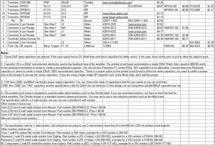
Audio Amplifier Section Parts List

Model 2800 single channel and bridge mode configuration.
Model 2800 schematic (modified AV800). Reference designators do not match the original AV800 schematic.
Protection circuit block diagram.
Protection circuit Controller

Protection
circuit Rail Detector 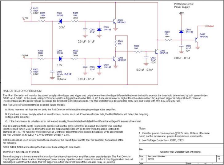
Protection circuit External Load Detector
Protection circuit DC offset
Protection circuit Output Short Detector
Protection circuit Clipping Detector
Protection circuit Speaker Relay
Protection circuit power supply.
Protection circuit Temperature Detector

Other Optional turn off muting (not included on PCB layout)
|
Politica de confidentialitate | Termeni si conditii de utilizare |

Vizualizari: 11115
Importanta: ![]()
Termeni si conditii de utilizare | Contact
© SCRIGROUP 2025 . All rights reserved