| CATEGORII DOCUMENTE |
| Bulgara | Ceha slovaca | Croata | Engleza | Estona | Finlandeza | Franceza |
| Germana | Italiana | Letona | Lituaniana | Maghiara | Olandeza | Poloneza |
| Sarba | Slovena | Spaniola | Suedeza | Turca | Ucraineana |
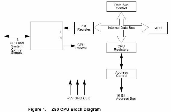
Z80 CPU architecture
The ZiLOG Z80 CPU family of components are fourth-generation enhanced microprocessors with exceptional computational power. They offer higher system throughput and more efficient memory utilization than comparable second- and third-generation microprocessors. The speed offerings from 620 MHz suit a wide range of applications which migrate software. The internal registers contain 208 bits of read/write memory that are accessible to the programmer. These registers include two sets of six general purpose registers which may be used individually as either 8-bit registers or as 16-bit register pairs. In addition, there are two sets of accumulator and flag registers.
The Z80 CPU also contains a Stack Pointer, Program Counter, two index registers, a REFRESH register, and an INTERRUPT register. The CPU is easy to incorporate into a system since it requires only a single +5V power source. All output signals are fully decoded and timed to control standard memory or peripheral circuits; the Z80 CPU is supported by an extensive family of peripheral controllers.
Figure 1 illustrates the internal architecture and major elements of the Z80 CPU:
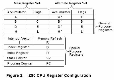
CPU Registers
The Z80 CPU contains 208 bits of R/W memory that are available to the programmer. Figure 2 illustrates how this memory is configured to eighteen 8-bit registers and four 16-bit registers. All Z80 registers are implemented using static RAM. The registers include two sets of six general-purpose registers that may be used individually as 8-bit registers or in pairs as 16-bit registers. There are also two sets of accumulator and flag registers and six special-purpose registers:
Special-Purpose Registers
Program Counter (PC)
The program counter holds the 16-bit address of the current instruction being fetched from memory. The PC is automatically incremented after its contents have been transferred to the address lines. When a program jump occurs, the new value is automatically placed in the PC, overriding the incrementer.
Stack Pointer (SP)
The stack pointer holds the 16-bit address of the current top of a stack located anywhere in external system RAM memory. The external stack memory is organized as a last-in first-out (LIFO) file. Data can be pushed into the stack from specific CPU registers or popped off of the stack to specific CPU registers through the execution of PUSH and POP instructions. The data popped from the stack is always the last data pushed into it. The stack allows simple implementation of multiple level interrupts, unlimited subroutine nesting and simplification of many types of data manipulation.
Two Index Registers (IX and IY)
The two independent index registers hold a 16-bit base address that is used in indexed addressing modes. In this mode, an index register is used as a base to point to a region in memory from which data is to be stored or retrieved. An additional byte is included in indexed instructions to specify a displacement from this base. This displacement is specified as a two's complement signed integer. This mode of addressing greatly simplifies many types of programs, especially where tables of data are used.
Interrupt Page Address Register (I)
The Z80 CPU can be operated in a mode where an indirect call to any memory location can be achieved in response to an interrupt. The I register is used for this purpose and stores the high order eight bits of the indirect address while the interrupting device provides the lower eight bits of the address. This feature allows interrupt routines to be dynamically located anywhere in memory with minimal access time to the routine.
Memory Refresh Register (R)
The Z80 CPU contains a memory refresh counter, enabling dynamic memories to be used with the same ease as static memories. Seven bits of this 8-bit register are automatically incremented after each instruction fetch. The eighth bit remains as programmed, resulting from an LD R, A instruction. The data in the refresh counter is sent out on the lower portion of the address bus along with a refresh control signal while the CPU is decoding and executing the fetched instruction. This mode of refresh is transparent to the programmer and does not slow the CPU operation. The programmer can load the R register for testing purposes, but this register is normally not used by the programmer. During refresh, the contents of the I register are placed on the upper eight bits of the address bus.
Accumulator and Flag Registers
The CPU includes two independent 8-bit accumulators and associated 8-bit flag registers. The accumulator holds the results of 8-bit arithmetic or logical
operations while the FLAG register indicates specific conditions for 8-bit or 16-bit operations, such as indicating whether or not the result of an operation is equal to zero. The programmer selects the accumulator and flag pair with a single exchange instruction so that it is possible to work with either pair.
General Purpose Registers
Two matched sets of general-purpose registers, each set containing six 8-bit registers, may be used individually as 8-bit registers or as 16-bit register pairs. One set is called BC, DE, and HL while the complementary set is called BC', DE', and HL'. At any one time, the programmer can select either set of registers to work through a single exchange command for the entire set. In systems that require fast interrupt response, one set of general purpose registers and an ACCUMULATOR/FLAG register may be reserved for handling this fast routine. One exchange command is executed to switch routines. This greatly reduces interrupt service time by eliminating the requirement for saving and retrieving register contents in the external stack during interrupt or subroutine processing. These general-purpose registers are used for a wide range of applications. They also simplify programing, specifically in ROM-based systems where little external read/write memory is available.
Arithmetic Logic Unit (ALU)
The 8-bit arithmetic and logical instructions of the CPU are executed in the ALU. Internally, the ALU communicates with the registers and the external data bus by using the internal data bus. Functions performed by the ALU include:
Add
Subtract
Logical AND
Logical OR
Logical Exclusive OR
Compare
Left or Right Shifts or Rotates (Arithmetic and Logical)
Increment
Decrement
Set Bit
Reset Bit
Test bit
Instruction Register and CPU Control
As each instruction is fetched from memory, it is placed in the INSTRUCTION register and decoded. The control sections performs this function and then generates and supplies the control signals necessary to read or write data from or to the registers, control the ALU, and provide required external control signals.
PIN DESCRIPTION
Overview
The Z80 CPU I/O pins are illustrated in Figure 3 and the function of each is described in the following paragraphs
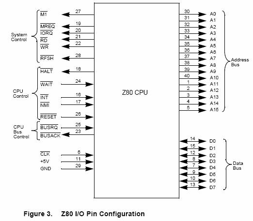
Pin Functions
A15A0
Address Bus (output, active High, tristate). A15-A0 form a 16-bit address bus. The Address Bus provides the address for memory data bus exchanges (up to 64 Kbytes) and for I/O device exchanges.
BUSACK
Bus Acknowledge (output,
active Low). Bus Acknowledge
indicates to the requesting device that the CPU address bus, data bus, and
control signals MREQ,
BUSREQ
Bus Request (input, active Low). Bus Request has a higher priority than NMI and is always recognized at the end of the current machine cycle. BUSREQ forces the CPU address bus, data bus, and control signals MREQ IORQ, RD, and WR to go to a high-impedance state so that other devices can control these lines. BUSREQ is normally wired-OR and requires an external pull-up for these applications. Extended BUSREQ periods due to extensive DMA operations can prevent the CPU from properly refreshing dynamic RAMS.
D7D0
Data Bus (input/output, active High, tristate). D7D0 constitute an 8-bit bidirectional data bus, used for data exchanges with memory and I/O.
HALT
INT
Interrupt Request (input, active Low). Interrupt Request is generated by I/O devices. The CPU honors a request at the end of the current instruction if the internal software-controlled interrupt enable flip-flop (IFF) is enabled. INT is normally wired-OR and requires an external pull-up for these applications.
IORQ
Input/Output Request (output, active Low, tristate). IORQ indicates that the lower half of the address bus holds a valid I/O address for an I/O read or write operation. IORQ is also generated concurrently with M1 during an interrupt acknowledge cycle to indicate that an interrupt response vector can
be placed on the data bus.
M1
Machine Cycle One (output, active Low). M1, together with MREQ, indicates that the current machine cycle is the opcode fetch cycle of an instruction execution. M1 together with IORQ, indicates an interrupt acknowledge cycle.
MREQ
emory Request (output, active Low, tristate). MREQ indicates that the address bus holds a valid address for a memory read of memory write operation.
NMI
Non-Maskable Interrupt (input, negative edge-triggered). NMI has a higher priority than INT. NMI is always recognized at the end of the current instruction, independent of the status of the interrupt enable flip-flop, and automatically forces the CPU to restart at location 0066H.
RD
Read (output, active Low, tristate). RD indicates that the CPU wants to read data from memory or an I/O device. The addressed I/O device or memory should use this signal to gate data into the CPU data bus.
RESET
Reset (input, active Low). RESET initializes the CPU as follows: it resets the interrupt enable flip-flop, clears the PC and registers I and R, and sets the interrupt status to Mode 0. During reset time, the address and data bus go to
a high-impedance state, and all control output signals go to the inactive state. Notice that RESET must be active for a minimum of three full clock cycles before the reset operation is complete.
RFSH
Refresh (output, active Low). RFSH, together with MREQ indicates that the lower seven bits of the systems address bus can be used as a refresh address to the systems dynamic memories.
WAIT
WAIT (input, active Low). WAIT communicates to the CPU that the addressed memory or I/O devices are not ready for a data transfer. The CPU continues to enter a WAIT state as long as this signal is active. Extended WAIT periods can prevent the CPU from properly refreshing dynamic memory.
WR
Write (output, active Low, tristate). WR indicates that the CPU data bus holds valid data to be stored at the addressed memory or I/O location.
CLKClock (input). Single-phase MOS-level clock.
TIMING
Overview
The Z80 CPU executes instructions by stepping through a precise set of basic operations. These include:
Memory Read or Write
I/O Device Read or Write
Interrupt Acknowledge
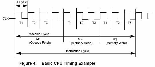
All instructions are series of basic operations. Each of these operations can take from three to six clock periods to complete or they can be lengthened to synchronize the CPU to the speed of external devices. The clock periods are referred to as T (time) cycles and the operations are referred to as M (machine) cycles. Figure 4 illustrates how a typical instruction is series of specific M and T cycles. Notice that this instruction consists of three machine cycles (M1, M2, and M3). The first machine cycle of any instruction is a fetch cycle which is four, five, or six T cycles long (unless lengthened by the WAIT signal, which is described in the next section). The fetch cycle (M1) is used to fetch the opcode of the next instruction to be executed. Subsequent machine cycles move data between the CPU and memory or I/O devices, and they may have anywhere from three to five T cycles (again, they may be lengthened by wait states to synchronize the external devices to the CPU). The following paragraphs describe the timing which occurs within any of the basic machine cycles. During T2 and every subsequent Tw, the CPU samples the WAIT line with the falling edge of Clock. If the WAIT line is active at this time, another WAIT state is entered during the following cycle. Using this technique, the read can be lengthened to match the access time of any type of memory device.
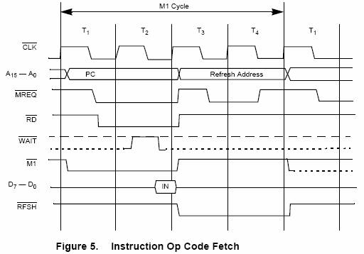
Instruction Fetch
Figure 5 depicts the timing during an M1 (opcode fetch) cycle. The PC is placed on the address bus at the beginning of the M1 cycle. One half clock cycle later the MREQ signal goes active. At this time the address to the memory has had time to stabilize so that the falling edge of MREQ can be used directly as a chip enable clock to dynamic memories. The RD line also goes active to indicate that the memory read data should be enabled into the CPU data bus. The CPU samples the data from the memory on the data bus with the rising edge of the clock of state T3 and this same edge is used by the CPU to turn off the RD and MREQ signals. Thus, the data has already been sampled by the CPU before the RD signal becomes inactive. Clock state T3 and T4 of a fetch cycle are used to refresh dynamic memories. The CPU uses this time to decode and execute the fetched instruction so that no other operation could be performed at this time. During T3 and T4, the lower seven bits of the address bus contain a memory refresh address and the RFSH signal becomes active indicating that a refresh read of all dynamic memories must be accomplished. An RD signal is not generated during refresh time to prevent data from different memory segments from being gated onto the data bus. The MREQ signal during refresh time should be used to perform a refresh read of all memory elements. The refresh signal can not be used by itself because the refresh address is only guaranteed to be stable during MREQ time.
Memory Read Or Write
Figure 6 illustrates the timing of memory read or write cycles other than an Op Code fetch cycle. These cycles are generally three clock periods long unless wait states are requested by the memory through the WAIT signal.
The MREQ signal and the RD signal are used the same as in the fetch cycle. In a memory write cycle, the MREQ also becomes active when the address bus is stable so that it can be used directly as a chip enable for dynamic memories. The WR line is active when data on the data bus is stable so that it can be used directly as a R/W pulse to virtually any type of semiconductor memory. Furthermore, the WR signal goes inactive one-half T state before the address and data bus contents are changed so that the overlap requirements for almost any type of semiconductor memory type is met.

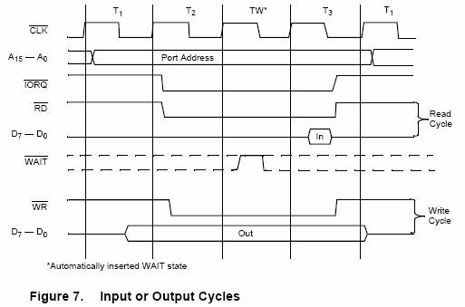
Input or Output Cycles
Figure 7 illustrates an I/O read or I/O write operation. During I/O operations a single wait state is automatically inserted. The reason is that during I/O operations, the time from when the IORQ signal goes active until the CPU must sample the WAIT line is very short. Without this extra state, sufficient time does not exist for an I/O port to decode its address and activate the WAIT line if a wait is required. Also, without this wait state, it is difficult to design MOS I/O devices that can operate at full CPU speed. During this wait state time, the WAIT request signal is sampled. During a read I/O operation, the RD line is used to enable the addressed port into the data bus just as in the case of a memory read. For I/O write operations, the WR line is used as a clock to the I/O port.
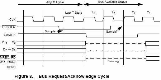
Bus Request/Acknowledge Cycle
Figure 8 illustrates the timing for a Bus Request/Acknowledge cycle. The BUSREQ signal is sampled by the CPU with the rising edge of the last clock period of any machine cycle. If the BUSREQ signal is active, the CPU sets its address, data, and tristate control signals to the high-impedance state with the rising edge of the next clock pulse. At that time, any external device can control the buses to transfer data between memory and I/O devices. (This operation is generally known as Direct Memory Access [DMA] using cycle stealing.). The maximum time for the CPU to respond to a bus request is the length of a machine cycle and the external controller can maintain control of the bus for as many clock cycles as is required. If very long DMA cycles are used, and dynamic memories are used, the external controller also performs the refresh function. This situation only occurs if very large blocks of data are transferred under DMA control. During a bus request cycle, the CPU cannot be interrupted by either an NMI or an INT signal.
Interrupt Request/Acknowledge Cycle
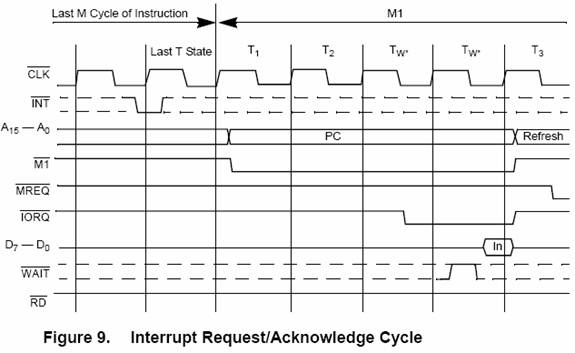
Figure 9 illustrates the timing associated with an interrupt cycle. The CPU samples the interrupt signal (INT) with the rising edge of the last clock at the end of any instruction. The signal is not accepted if the internal CPU software controlled interrupt enable flip-flop is not set or if the BUSREQ signal is active. When the signal is accepted, a special M1 cycle is generated. During this special M1 cycle, the IORQ signal becomes active (instead of the normal MREQ) to indicate that the interrupting device can place an 8-bit vector on the data bus. Two wait states are automatically added to this cycle. These states are added so that a ripple priority interrupt scheme can be easily implemented. The two wait states allow sufficient time for the ripple signals to stabilize and identify which I/O device must insert the response vector. Refer to Chapter 6 for details on how the interrupt response vector is utilized by the CPU
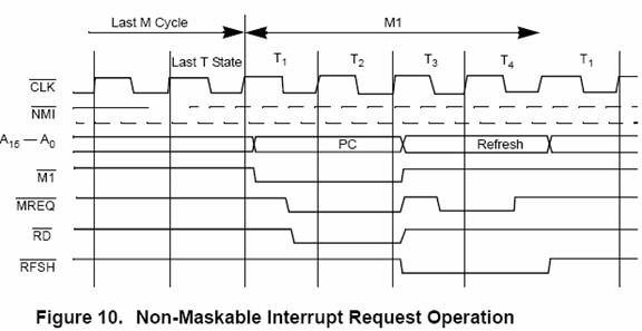
Non-Maskable Interrupt Response
Figure 10 illustrates the request/acknowledge cycle for the non-maskable interrupt. This signal is sampled at the same time as the interrupt line, but this line takes priority over the normal interrupt and it can not be disabled under software control. Its usual function is to provide immediate response to important signals such as an impending power failure. The CPU response to a non-maskable interrupt is similar to a normal memory read operation. The only difference is that the content of the data bus is ignored while the processor automatically stores the PC in the external stack and jumps to location 0066H. The service routine for the non-maskable interrupt must begin at this location if this interrupt is used.
HALT Exit
Whenever a software HALT instruction is executed, the CPU executes NOPs until an interrupt is received (either a non-maskable or a maskable interrupt while the interrupt flip-flop is enabled). The two interrupt lines are sampled with the rising clock edge during each T4 state as depicted in Figure 11. If a non-maskable interrupt has been received or a maskable interrupt has been received and the interrupt enable flip-flop is set, then the
HALT state is exited on the next rising clock edge. The following cycle is an interrupt acknowledge cycle corresponding to the type of interrupt that was received. If both are received at this time, then the non-maskable one is acknowledged since it has highest priority. The purpose of executing NOP instructions while in the HALT state is to keep the memory refresh signals active. Each cycle in the HALT state is a normal M1 (fetch) cycle except that the data received from the memory is ignored and a NOP instruction is forced internally to the CPU. The HALT acknowledge signal is active during this time indicating that the processor is in the HALT state.

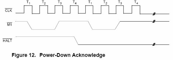
Power-Down Acknowledge Cycle
When the clock input to the CMOS Z80 CPU is stopped at either a High or Low level, the CMOS Z80 CPU stops its operation and maintains all registers and control signals. However, ICC2 (standby supply current) is guaranteed only when the system clock is stopped at a Low level during T4 of the machine cycle following the execution of the HALT instruction. The timing diagram for the power-down function, when implemented with the HALT instruction, is shown in Figure 12.
Power-Down Release Cycle
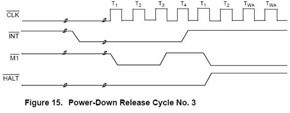
The system clock must be supplied to the CMOS Z80 CPU to release the power-down state. When the system clock is supplied to the CLK input, the CMOS Z80 CPU restarts operations from the point at which the power-down state was implemented. The timing diagrams for the release from power down mode are featured in Figure 13, 14 and 15.
When the HALT instruction is executed to enter the power-down state, the CMOS Z80 CPU also enters the HALT state. An interrupt signal (either NMI or ANT) or a RESET signal must be applied to the CPU after the system clock is supplied in order to release the power-down state.

INTERRUPT RESPONSE
Overview
An interrupt allows peripheral devices to suspend CPU operation and force the CPU to start a peripheral service routine. This service routine usually involves the exchange of data, status, or control information between the CPU and the peripheral. When the service routine is completed, the CPU returns to the operation from which it was interrupted.
Interrupt Enable/Disable
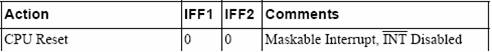
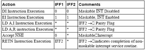
The Z80 CPU has two interrupt inputs, a software maskable interrupt (INT) and a non-maskable interrupt (NMI). The non-maskable interrupt cannot be disabled by the programmer and is accepted whenever a peripheral device requests it. This interrupt is generally reserved for very important functions that can be enabled or disabled selectively by the programmer. This routine allows the programmer to disable the interrupt during periods when his program has timing constraints that do not allow interrupt. In the Z80 CPU, there is an interrupt enable flip-flop (IFF) that is set or reset by the programmer using the Enable Interrupt (EI) and Disable Interrupt (DI) instructions. When the IFF is reset, an interrupt cannot be accepted by the CPU.
The two enable flip-flops are IFF1 and IFF2.
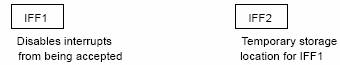
The state of IFF1 is used to inhibit interrupts while IFF2 is used as a temporary storage location for IFF1.
A CPU reset forces both the IFF1 and IFF2 to the reset state, which disables interrupts. Interrupts can be enabled at any time by an EI instruction from the programmer. When an EI instruction is executed, any pending interrupt request is not accepted until after the instruction following EI is executed.
This single instruction delay is necessary when the next instruction is a return instruction. Interrupts are not allowed until a return is completed. The EI instruction sets both IFF1 and IFF2 to the enable state. When the CPU accepts a maskable interrupt, both IFF1 and IFF2 are automatically reset, inhibiting further interrupts until the programmer issues a new El instruction. Note that for all of the previous cases, IFF1 and IFF2 are always equal.
The purpose of IFF2 is to save the status of IFF1 when a non-maskable interrupt occurs. When a non-maskable interrupt is accepted, IFF1 resets to prevent further interrupts until reenabled by the programmer. Thus, after a non-maskable interrupt is accepted, maskable interrupts are disabled but the previous state of IFF1 has been saved so that the complete state of the CPU just prior to the non-maskable interrupt can be restored at any time. When a Load Register A with Register I (LD A, I) instruction or a Load Register A with Register R (LD A, R) instruction is executed, the state of IFF2 is copied to the parity flag where it can be tested or stored.
A second method of restoring the status of IFF1 is through the execution of a Return From Non-Maskable Interrupt (RETN) instruction. This instruction indicates that the non-maskable interrupt service routine is complete and the contents of IFF2 are now copied back into IFF1 so that the status of IFF1 just prior to the acceptance of the non-maskable interrupt is restored automatically.
Table 2 is a summary of the effect of different instructions on the two enable
flip-flops
Table 2. Interrupt Enable/Disable, Flip-Flops
CPU Response
Non-Maskable
The CPU always accepts a non-maskable interrupt. When this occurs, the CPU ignores the next instruction that it fetches and instead performs a restart to location 0066H. The CPU functions as if it had recycled a restart instruction, but to a location other than one of the eight software restart locations. A restart is merely a call to a specific address in page 0 of memory.
The CPU can be programmed to respond to the maskable interrupt in any one of three possible modes:
Mode 0
This mode is similar to the 8080A interrupt response mode. With this mode, the interrupting device can place any instruction on the data bus and the CPU executes it. Thus, the interrupting device provides the next instruction to be executed. Often this is a restart instruction because the interrupting device only need supply a single byte instruction. Alternatively, any other instruction such as a 3-byte call to any location in memory could be executed.
The number of clock cycles necessary to execute this instruction is two more than the normal number for the instruction. This occurs because the CPU automatically adds two wait states to an Interrupt response cycle to allow sufficient time to implement an external daisy-chain for priority control. Figure 9 and Figure 10 illustrate the detailed timing for an interrupt response. After the application of RESET, the CPU automatically enters interrupt Mode 0.
Mode 1
When this mode is selected by the programmer, the CPU responds to an interrupt by executing a restart to location 0038H. Thus, the response is identical to that for a non-maskable interrupt except that the call location is 0038H instead of 0066H. The number of cycles required to complete the restart instruction is two more than normal due to the two added wait states.
Mode 2
This mode is the most powerful interrupt response mode. With a single 8-bit byte from the user, an indirect call can be made to any memory location. In this mode, the programmer maintains a table of 16-bit starting addresses for every interrupt service routine. This table may be located anywhere in memory. When an interrupt is accepted, a 16-bit pointer must be formed to obtain the desired interrupt service routine starting address from the table.
The upper eight bits of this pointer is formed from the contents of the I register. The I register must be loaded with the applicable value by the programmer, such as LD I, A. A CPU reset clears the I register so that it is initialized to zero. The lower eight bits of the pointer must be supplied by the interrupting device. Only seven bits are required from the interrupting device because the least-significant bit must be a zero. This is required because the pointer is used to get two adjacent bytes to form a complete 16- bit service routine starting address and the addresses must always start in even locations.
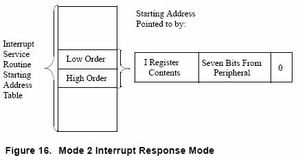
The first byte in the table is the least-significant (low order portion of the address). The programmer must complete this table with the correct addresses before any interrupts are accepted.
The programmer can change this table by storing it in Read/Write Memory, which also allows individual peripherals to be serviced by different service routines.
When the interrupting device supplies the lower portion of the pointer, the CPU automatically pushes the program counter into the stack, obtains the starting address from the table, and performs a jump to this address. This mode of response requires 19 clock periods to complete (seven to fetch the lower eight bits from the interrupting device, six to save the program counter, and six to obtain the jump address).
The Z80 peripheral devices include a daisy-chain priority interrupt structure that automatically supplies the programmed vector to the CPU during interrupt acknowledge.
Z80 CPU Instruction Description
The Z80 CPU can execute 158 different instruction types including all 78 of the 8080A CPU. The instructions fall into these major groups:
Load and Exchange
Block Transfer and Search
Arithmetic and Logical
Rotate and Shift
Bit Manipulation (Set, Reset, Test)
Jump, Call, and Return
Input/Output
Basic CPU Control
Instruction Types
The load instructions move data internally among CPU registers or between CPU registers and external memory. All these instructions specify a source location from which the data is to be moved and a destination location. The source location is not altered by a load instruction. Examples of load group instructions include moves between any of the general-purpose registers such as move the data to register B from register C. This group also includes load-immediate to any CPU register or to any external memory location. Other types of load instructions allow transfer between CPU registers and memory locations. The exchange instructions can trade the contents of two registers.
A unique set of block transfer instructions is provided in the Z80. With a single instruction, a block of memory of any size can be moved to any other location in memory. This set of block moves is extremely valuable when processing large strings of data. With a single instruction, a block of external memory of any desired length can be searched for any 8-bit character. When the character is found or the end of the block is reached, the instruction automatically terminates. Both the block transfer and the block search instructions can be interrupted during their execution so they do not occupy the CPU for long periods of time.
The arithmetic and logical instructions operate on data stored in the accumulator and other general-purpose CPU registers or external memory locations. The results of the operations are placed in the accumulator and the appropriate flags are set according to the result of the operation.
An example of an arithmetic operation is adding the accumulator to the contents of an external memory location. The results of the addition are placed in the accumulator. This group also includes 16-bit addition and subtraction between 16-bit CPU registers.
The rotate and shift group allows any register or any memory location to be rotated right or left, with or without carry either arithmetic or logical.
Also, a digit in the accumulator can be rotated right or left with two digits in any memory location.
The bit manipulation instructions allow any bit in the accumulator, any general-purpose register, or any external memory location to be set, reset, or tested with a single instruction. For example, the most-significant bit of register H can be reset. This group is especially useful in control applications and for controlling software flags in general-purpose programming.
The JUMP, CALL, and RETURN instructions are used to transfer between various locations in the users program. This group uses several different techniques for obtaining the new program counter address from specific external memory locations. A unique type of call is the RESTART instruction. This instruction actually contains the new address as a part of the 8-bit Op Code. This is possible because only eight separate addresses located in page zero of the external memory may be specified. Program jumps may also be achieved by loading register HL, IX, or IY directly into the PC, thus allowing the jump address to be a complex function of the routine being executed.
The input/output group of instructions in the Z80 allow for a wide range of transfers between external memory locations or the general-purpose
CPU registers, and the
external I/O devices. In each case, the port number is provided on the lower
eight bits of the address bus during any I/O transaction. One instruction
allows this port number to be specified by the second byte of the instruction
while other Z80 instructions allow it to be specified as the content of the C
register. One major advantage of using the C register as a pointer to the I/O
device is that it allows multiple I/O ports to share common software driver
routines. This advantage is not possible when the address is part of the Op
Code if the routines are stored in
The Z80 CPU includes single instructions that can move blocks of data (up to 256 bytes) automatically to or from any I/O port directly to any memory location. In conjunction with the dual set of general-purpose registers, these instructions provide fast I/O block transfer rates. The power of this I/O instruction set is demonstrated by the Z80 CPU providing all required floppy disk formatting on double-density floppy disk drives on an interrupt-driven basis. For example, the CPU provides the preamble, address, data, and enables the CRC codes.
Finally, the basic CPU control instructions allow various options and modes. This group includes instructions such as setting or resetting the interrupt enable flip-flop or setting the mode of interrupt response.
Addressing Modes
Most of the Z80 instructions operate on data stored in internal CPU registers, external memory, or in the I/O ports. Addressing refers to how the address of this data is generated in each instruction. This section is a brief summary of the types of addressing used in the Z80 while subsequent sections detail the type of addressing available for each instruction group.
Immediate
In this mode of addressing, the byte following the Op Code in memory contains the actual operand

Examples of this type of instruction is loading the accumulator with a constant, where the constant is the byte immediately following the Op Code.
Immediate Extended
This mode is an extension of immediate addressing in that the two bytes following the Op Codes are the operand.
Examples of this type of instruction is loading the HL register pair (16-bit register) with 16 bits (two bytes) of data.
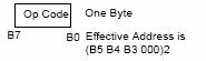
Modified Page Zero Addressing
The Z80 has a special single byte CALL instruction to any of eight locations in page zero of memory. This instruction, which is referred to as a restart, sets the PC to an effective address in page zero. The value of this instruction is that it allows a single byte to specify a complete 16-bit address where commonly called subroutines are located, thus saving memory space.
Relative Addressing
Relative addressing uses one byte of data following the Op Code to specify a displacement from the existing program to which a program jump can occur. This displacement is a signed twos complement number that is added to the address of the Op Code of the following instruction.
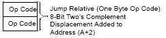
The value of relative addressing is that it allows jumps to nearby locations while only requiring two bytes of memory space. For most programs, relative jumps are by far the most prevalent type of jump due to the proximity of related program segments. Thus, these instructions can Significantly reduce memory space requirements. The signed displacement can range between +127 and -128 from A+2. This allows for a total displacement of +129 to -126 from the jump relative Op Code address. Another major advantage is that it allows for relocatable code.
Extended Addressing
Extended Addressing provides for two bytes (16 bits) of address to be included in the instruction. This data can be an address to which a program can jump or it can be an address where an operand is located.

Extended addressing is required for a program to jump from any location in memory to any other location, or load and store data in any memory location. During extended addressing use, specify the source or destination address of an operand. This notation (nn) is used to indicate the content of memory at nn, where nn is the 16-bit address specified in the instruction. The two bytes of address nn are used as a pointer to a memory location. The use of the parentheses always means that the value enclosed within them is used as a pointer to a memory location. For example, (3200) refers to the contents of memory at location 1200.
Indexed Addressing
In this type of addressing, the byte of data following the Op Code contains a displacement that is added to one of the two index registers (the Op Code specifies which index register is used) to form a pointer to memory. The contents of the index register are not altered by this operation.

An example of an indexed instruction is to load the contents of the memory location (Index Register + Displacement) into the accumulator.
The displacement is a signed twos complement number. Indexed addressing greatly simplifies programs using tables of data because the index register can point to the start of any table. Two index registers are provided because very often operations require two or more tables.
Indexed addressing also allows for relocatable code.
The two index registers in the Z80 are referred to as IX and IY. To indicate indexed addressing the notation use:
(IX+d) or (IY+d)
Here is the displacement specified after the Op Code. The parentheses indicate that this value is used as a pointer to external memory.
Register Addressing
Many of the Z80 Op Codes contain bits of information that specify which
CPU register is to be used for an operation. An example of register addressing is to load the data in register 6 into register C.
Implied Addressing
Implied addressing refers to operations where the Op Code automatically implies one or more CPU registers as containing the operands. An example is the set of arithmetic operations where the accumulator is always implied to be the destination of the results.
Register Indirect Addressing
This type of addressing specifies a 16-bit CPU register pair (such as HL) to be used as a pointer to any location in memory. This type of instruction is very powerful and it is used in a wide range of applications.
![]()
An example of this type of instruction is to load the accumulator with the data in the memory location pointed to by the HL register contents.
Indexed addressing is actually a form of register indirect addressing except that a displacement is added with indexed addressing. Register indirect addressing allows for very powerful but simple to implement memory accesses. The block move and search commands in the Z80 are extensions of this type of addressing where automatic register incrementing, decrementing, and comparing has been added. The notation for indicating register indirect addressing is to put parentheses around the name of the register that is to be used as the pointer. For example, the symbol (HL) specifies that the contents of the HL register are to be used as a pointer to a memory location. Often register indirect addressing is used to specify 16-bit operands. In this case, the register contents point to the lower order portion of the operand while the register contents are automatically incremented to obtain the upper portion of the operand.
Bit Addressing
The Z80 contains a large number of bit set, reset, and test instructions.
These instructions allow any memory location or CPU register to be specified for a bit operation through one of three previous addressing modes (register, register indirect, and indexed) while three bits in the Op Code specify which of the eight bits is to be manipulated.
Addressing Mode Combinations
Many instructions include more than one operand (such as arithmetic instructions or loads). In these cases, two types of addressing may be employed. For example, load can use immediate addressing to specify the source and register indirect or indexed addressing to specify the destination.
Z80 Instruction Set
Z80 Assembly Language
The assembly language allows the user to write a program without concern for memory addresses or machine instruction formats. It uses symbolic addresses to identify memory locations and mnemonic codes (Op Codes and operands) to represent the instructions. Labels (symbols) are assigned to a particular instruction step in a source program to identify that step as an entry point for use in subsequent instructions. Operands following each instruction represent storage locations, registers, or constant values. The assembly language also includes assembler directives that supplement the machine instruction. A pseudo-op, for example, is a statement that is not translated to a machine instruction, but rather is interpreted as a directive that controls the assembly process.
A program written in assembly language is called a source program, which consists of symbolic commands called statements. Each statement is written on a single line and may consist of from one to four entries: A label field, an operation field, an operand field, and a comment field. The source program is processed by the assembler to obtain a machine language program (object program) that can be executed directly by the Z80 CPU.
ZiLOG provides several assemblers that differ in the features offered.
Both absolute and relocatable assemblers are available with the Development
and Micro-computer Systems. The absolute assembler is contained in base level
software operating in a 16K memory space, while the relocating assembler is
part of the
Z80 Status Indicator Flags
The flag registers (F and F') supply information to the user about the status of the Z80 at any given time. The bit positions for each flag is listed below:

Each of the two flag registers contains 6 bits of status information that are set or cleared by CPU operations. (Bits 3 and 5 are not used.) Four of these bits (C, P/V, Z, and S) may be tested for use with conditional JUMP, CALL, or RETURN instructions. Two flags may not be tested (H, N) and are used for BCD arithmetic.
Carry Flag
The Carry Flag (C) is set or cleared depending on the operation performed.
For ADD instructions that generate a Carry, and SUB instructions that generate a Borrow, the Carry Flag sets. The Carry Flag is reset by an ADD instruction that does not generate a Carry, and by a SUB instruction that does not generate a Borrow. This saved Carry facilitates software routines for extended precision arithmetic. Also, the DAA instruction sets the Carry Flag if the conditions for making the decimal adjustment are met.
For instructions RLA,
RRA, RLS, and RRS, the Carry bit is used as a link between the least
significant byte (LSB) and most significant byte (MSB) for any register or
memory location. During instructions RLCA, RLC, and
For the logical instructions AND, OR, and XOR, the Carry is reset.
The Carry Flag can also be set by the Set Carry Flag (SCF) and complemented by the Compliment Carry Flag (CCF) instructions.
Add/Subtract Flag
The Add/Subtract Flag (N) is used by the Decimal Adjust Accumulator instruction (DAA) to distinguish between ADD and SUB instructions. For ADD instructions, N is cleared to 0. For SUB instructions, N is set to 1.
Add/Subtract Flag
The Decimal Adjust Accumulator instruction (DAA) uses this flag to distinguish between ADD and SUBTRACT instructions. For all ADD instructions, N sets to 0. For all SUBTRACT instructions, N sets to 1.
Parity/Overflow Flag (P/V)
This flag is set to a specific state depending on the operation performed.
For arithmetic operations, this flag indicates an Overflow condition when the result in the Accumulator is greater than the maximum possible number (+127) or is less than the minimum possible number (128). This Overflow condition is determined by examining the sign bits of the operands.
For addition, operands with different signs never cause Overflow. When adding operands with like signs and the result has a different sign, the Overflow Flag is set, for example:
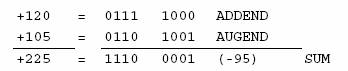
The two numbers added together resulted in a number that exceeds +127 and the two positive operands have resulted in a negative number (-95), which is incorrect. The Overflow Flag is therefore set.
For subtraction, Overflow can occur for operands of unlike signs. Operands of like signs never cause Overflow. For example:
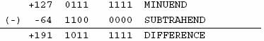
The minuend sign has changed from a Positive to a negative, giving an incorrect difference. Overflow is set.
Another method for identifying an Overflow is to observe the Carry to and out of the sign bit. If there is a Carry in and no Carry out, or if there is no Carry in and a Carry out, then Overflow has occurred.
This flag is also used with logical operations and rotate instructions to indicate the resulting parity is Even. The number of 1 bits in a byte are counted. If the total is Odd, ODD parity is flagged (P = 0). If the total is Even, EVEN parity is flagged (P = 1).
During search instructions (CPI, CPIR, CPD, CPDR) and block transfer instructions (LDI, LDIR, LDD, LDDR), the P/V Flag monitors the state of the Byte Count Register (BC).When decrementing, if the byte counter decrements to 0, the flag is cleared to 0, otherwise the flag is set to1.
During LD A, I and LD A, R instructions, the P/V Flag is set with the value of the interrupt enable flip-flop (IFF2) for storage or testing.
When inputting a byte from an I/O device with an IN r, (C), instruction, the P/V Flag is adjusted to indicate the data parity.
Half Carry Flag
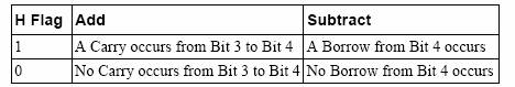
The Half-Carry Flag (H) is set (1) or cleared (0) depending on the Carry and Borrow status between Bits 3 and 4 of an 8-bit arithmetic operation.
This flag is used by the Decimal Adjust Accumulator instruction (DAA) to correct the result of a packed BCD add or subtract operation. The H Flag is set (1) or cleared (0) according to the following table:
Zero Flag
The Zero Flag (Z) is set (1) or cleared (0) if the result generated by the execution of certain instructions is 0.
For 8-bit arithmetic and logical operations, the Z flag is set to a 1 if the resulting byte in the Accumulator is 0. If the byte is not 0, the Z flag is reset to 0.
For compare (Search) instructions, the Z flag is set to 1 if the value in the Accumulator is equal to the value in the memory location indicated by the value of the Register pair HL.
When testing a bit in a register or memory location, the Z flag contains the complemented state of the indicated bit (see Bit b, s).
When inputting or outputting a byte between a memory
location and an I/O device (
Sign Flag
The Sign Flag (S) stores the state of the most-significant bit of the Accumulator (bit 7). When the Z80 performs arithmetic operations on signed numbers, the binary twos-complement notation is used to represent and process numeric information. A positive number is identified by a 0 in Bit 7. A negative number is identified by a 1. The binary equivalent of the magnitude of a positive number is stored in bits 0 to 6 for a total range of from 0 to 127. A negative number is represented by the twos complement of the equivalent positive number. The total range for negative numbers is from 1 to 128.
When inputting a byte from an I/O device to a register using an IN r, (C) instruction, the S Flag indicates either positive (S = 0) or negative (S = 1) data.
Clasa 1. Instructiuni de transfer de 8 biti LOAD-8
Mnemonici incluse: LD
Totalul intructiunilor din clasa: 111
Numarul de grupe: 11
Clasa 2. Instructiuni de transfer de 16 biti LOAD-16
Mnemonici incluse: LD, EX, EXX, POP, PUSH
Totalul instructiunilor din clasa: 39
Numarul de grupe: 10
Clasa 3 Instructiuni de transfer de blocuri de date LOAD-IDR
Mnemonici incluse: LDD, LDDR, LDI, LDIR
Totalul instructiunilor din clasa: 4
Numarul de grupe: 2
Clasa 4. Instructiuni aritmetice/logice pe 8 biti AR/LOG-8
Mnemonici incluse: ADD, ADC, SUB, SBC, AND, XOR, OR, CP, INC, DEC, CPL, NEG, DAA, RLCA, RRCA, RLA, RRA
Totalul instructiunilor din clasa: 115
Numarul de grupe: 26
Clasa 5. Instructiuni aritmetice de 16 biti ARIT-16
Mnemonici incluse: ADD, ADC, BC, INC, DEC
Totalul instructiunilor din clasa: 32
Numarul de grupe: 7
Clasa 6. Instructiuni logice pe blocuri de date LOG-IDR
Mnemonici incluse: CPD, CPDR, CPI, CPIR
Totalul instructiunilor din clasa: 4
Numarul de grupe: 2
Clasa 7. Instructiuni orientate pe bit BITSR
Mnemonici incluse: BIT, SET, RES, SCF, CCF
Totalul instructiunilor din clasa: 242
Numarul de grupe: 7
Clasa 8. Instructiuni de salt JUMP
Mnemonici incluse: JP, JR, DJNZ
Totalul instructiunilor din clasa: 18
Numarul de grupe: 6
Clasa 9. Instructiuni de apel si revenire din subrutina CALL/RET
Mnemonici incluse: CALL, RET, RST
Totalul instructiunilor din clasa: 26
Numarul de grupe: 5
Clasa 10. Instructiuni de rotire si deplasare ROT/HIFT
Mnemonici incluse: RLC, RRC,RL, RR, SLA, SRA, SRL, RLD, RRD
Totalul instructiunilor din clasa: 72
Numarul de grupe: 9
Clasa 11. Instructiuni de intrare/ iesire IN/OUT
Mnemonici incluse: IN, IND, INDR, INI, INIR, OTDR, OTIR, AUT, OUTD
Totalul instructiunilor din clasa: 24
Numarul de grupe: 8
Clasa 12. Instructiuni de comanda SYS
Mnemonici incluse: DI, EI, HALT, IM, NOP, RETI, RETN
Totalul intructiunilor din clasa: 9
Numarul de grupe: 5
|
Politica de confidentialitate | Termeni si conditii de utilizare |

Vizualizari: 4652
Importanta: ![]()
Termeni si conditii de utilizare | Contact
© SCRIGROUP 2026 . All rights reserved