| CATEGORII DOCUMENTE |
| Bulgara | Ceha slovaca | Croata | Engleza | Estona | Finlandeza | Franceza |
| Germana | Italiana | Letona | Lituaniana | Maghiara | Olandeza | Poloneza |
| Sarba | Slovena | Spaniola | Suedeza | Turca | Ucraineana |
Analysis
of the parasitic devices in bipolar IC technology
supported by TCAD modeling and simulation
Abstract. The implementation of TCAD process and device simulation of electrical properties of bipolar transistor cell for extraction of its equivalent circuit is presented. A unique insight into the internal transistor structure operation allows for analysis of the critical regions and for better understanding of the electro-physical behaviour of bipolar transistor. Very good agreement of simulated electrical characteristics by TCAD as well as SPICE equivalent circuit model with experimental ones confirms the validity of the derived model. The sudden increase of substrate current is caused by a parasitic lateral PNP transistor which emitter under certain circumstances becomes forward biased. The influence of temperature on the electrical properties of bipolar transistor is analysed also. The advantage and efficiency of the implementation of various simulation tools, particularly process and device simulators for better understanding of the properties of semiconductor devices is clearly seen.
The increasing on-chip circuit and system integration allowed by continuing miniaturization of individual semiconductor devices, which are approaching their physical limits, generate a strong pressure on better understanding of the electro-physical behaviour of individual semiconductor structures integrated in IC technology [1]. Although the system level approach is the main stream in new technologies, the deep understanding of physical behaviour of operation of basic semiconductor devices and building blocks provides the system engineers with necessary background for exploitation of the maximum performance from a given technology. The massive implementation of advanced design software tools with large libraries of different cells as well as advanced simulators based on numerical modelling and simulation of fabrication processes, electronic devices and circuits play an increasingly important role in industrial practice [2].
An example of the implementation of TCAD process and device simulators for modelling and simulation of the NPN bipolar transistor with buried collector and reverse biased p-n junction isolation in the common emitter configuration is presented. It allows interpreting the electrical characteristics, e.g. the Gummel plot by the knowledge of internal electro-physical properties of the structure profile of bipolar transistor as potential distribution, hole density and hole current density.
The model structure of the bipolar transistor fabricated in technology with buried collector and reverse biased p-n junction isolation which corresponds to the real bipolar IC technology was designed and simulated by 2-D process simulation in ISE TCAD process simulator DIOS [3] (Fig. 1.). The ntype epitaxial layer was grown on p-type substrate into which the n+-type buried collector and p+type region for p-type isolation ring were implanted prior to epitaxial growth.
The sequence of ion implantation steps in predefined regions consisting p-type isolation ring, ptype base and n+-type emitter and collector planar contact followed by high temperature activation of impurities create the bipolar transistor structure as basic building block of bipolar IC technology. Planar ohmic contacts to emitter, base, collector and substrate for applying external voltages were defined.
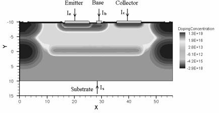
Fig. 1. Schematic of the structure of bipolar transistor
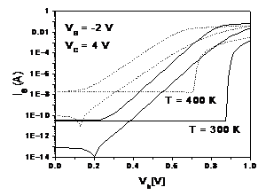
The very good qualitative agreement of the simulated and measured static I-V characteristics of the model structure of bipolar NPN transistor in the common emitter configuration, namely base, collector, and substrate currents Ib, Ic, and Is are shown on Fig. 2.
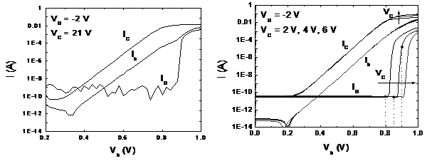
Fig. 2. Measured and simulated Gummel plot of bipolar transistor
The internal properties of the analyzed structure are in Fig. 3. It can be clearly seen that due to an increasing voltage drop on series collector resistance the base-collector junction on the left side of analyzed structure is forward bias and injects holes from p-type base to n-type collector. These holes are then swept by the reverse biased p-n junction created by p-type isolation ring and n-type collector and large hole current flows to substrate. Such behaviour corresponds to the creation of the parasitic lateral PNP bipolar transistor.
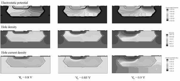
Fig. 3. The distributions of potential, free holes and hole current density
Using the unique insight into the operation of the NPN bipolar transistor cell structure provided by the above TCAD analysis the equivalent circuit model for SPICE simulation was derived (Fig. 4.). The bipolar technology with buried collector and reverse biased p-type isolation junction may be modelled by the vertical active NPN bipolar transistor including its base and collector series resistances and lateral parasitic PNP bipolar transistor which is merged with the active transistor. The p-type base of active vertical transistor creates the p-type emitter of parasitic transistor, n-type collector of the active vertical transistor is n-type base of the parasitic lateral transistor and p-type isolation guard ring and substrate create the collector of the parasitic lateral transistor.
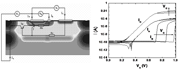
Fig. 4. Equivalent circuit model of the NPN bipolar transistor for SPICE simulation and the IV characteristics simulated by SPICE
The base and collector currents of active NPN transistor increase with base voltage Vb. At certain Vb the voltage drop on series Rc resistance forward biases the normally reversed biased collector junction of the NPN transistor on left side of the analyzed transistor cell. The amplifying effect of this parasitic lateral PNP bipolar transistor can be then considered as the origin of the sudden super-exponential growth of the substrate current at high base voltage Vb.
The parameters of the individual elements of the derived model (input netlist) were extracted either from the 2-D simulation. The qualitative agreement of the simulated I-V characteristics with the experimental results as well as the simulated characteristics from 2-D device simulation confirms the validity of our approach.
 Influence of temperature
The influence of the temperature on the transistor behaviour and properties is shown in Fig. 5. With increasing device temperature the base-emitter diffusion (built-in) voltage decreases and the base and collector currents increase at smaller base voltage Vb. As a consequence the voltage drop on the series collector resistance also increases and a dramatic increase of substrate current occurs at lower Vb with increasing temperature.
Fig. 5. Influence of device temperature on substrate current
The 2-D numerical process and device modeling and simulation were presented as the very effective tools for the better understanding of internal behavior of complex semiconductor structures and so for the physical interpretation of the experimental electrical characteristics of analyzed equivalent semiconductor structures. The equivalent circuit of the NPN bipolar transistor cell with characteristic parameters of the individual elements was derived based on the knowledge of the internal properties of the analyzed structure and verified by SPICE simulation.
The visualization of internal electro-physical properties of analyzed structure which cannot be directly measured as potential, carrier densities, electron and hole currents, impact ionization and others and their correlation with output electrical characteristics is extremely useful for physical interpretation of obtained data. The user with some expertise can analyze the critical points and regions and extract the parasitic effects.
References
DE M, H., Demands on Microelectronics education and Research in Post
PC Area,
Proceedings of the 3rd EWME,
pp. 9 - 14, Kluwer Academic Publishers, Dordrecht 2000
BRADLEY, B. S., Principles vs. Practices in
Undergraduate Microelectronics Systems
Education, In: Proceedings
of MSE01, pp. 22-23, Las Vegas 2001
ISE DIOS and DESSIS, User manual, ver. 9.5, ISE Zurich, Switzerland
|
Politica de confidentialitate | Termeni si conditii de utilizare |

Vizualizari: 2397
Importanta: ![]()
Termeni si conditii de utilizare | Contact
© SCRIGROUP 2026 . All rights reserved