Scrigroup - Documente si articole

Username / Parola inexistente      

Home Documente Upload Resurse Alte limbi doc  
BulgaraCeha slovacaCroataEnglezaEstonaFinlandezaFranceza
GermanaItalianaLetonaLituanianaMaghiaraOlandezaPoloneza
SarbaSlovenaSpaniolaSuedezaTurcaUcraineana

AdministrationAnimalsArtBiologyBooksBotanicsBusinessCars
ChemistryComputersComunicationsConstructionEcologyEconomyEducationElectronics
EngineeringEntertainmentFinancialFishingGamesGeographyGrammarHealth
HistoryHuman-resourcesLegislationLiteratureManagementsManualsMarketingMathematic
MedicinesMovieMusicNutritionPersonalitiesPhysicPoliticalPsychology
RecipesSociologySoftwareSportsTechnicalTourismVarious

The Basic System Components

computers


+ Font mai mare | - Font mai mic


The Basic System Components

The basic operational design of a computer system is called its architecture. John Von Neumann, a pioneer in computer design, is given credit for the architecture of most computers in use today. For example, the 80x86 family uses the Von Neumann architecture (VNA). A typical Von Neumann system has three major components: the central processing unit (or CPU), memory, and input/output (or I/O). The way a system designer combines these components impacts system performance:

In VNA machines, like the 80x86 family, the CPU is where all the action takes place. All computations occur inside the CPU. Data and CPU instructions reside in memory until required by the CPU. To the CPU, most I/O devices look like memory because the CPU can store data to an output device and read data from an input device. The major difference between memory and I/O locations is the fact that I/O locations are generally associated with external devices in the outside world.

1.1 The System Bus

The system bus connects the various components of a VNA machine. The 80x86 family has three major busses: the address bus, the data bus, and the control bus. A bus is a collection of wires on which electrical signals pass between components in the system. These busses vary from processor to processor. However, each bus carries comparable information on all processors; e.g., the data bus may have a different implementation on the 80386 than on the 8088, but both carry data between the processor, I/O, and memory.

A typical 80x86 system component uses standard TTL logic levels. This means each wire on a bus uses a standard voltage level to represent zero and one. We will always specify zero and one rather than the electrical levels because these levels vary on different processors (especially laptops).

1.1.1 The Data Bus

The 80x86 processors use the data bus to shuffle data between the various components in a computer system. The size of this bus varies widely in the 80x86 family. Indeed, this bus defines the 'size' of the processor.

On typical 80x86 systems, the data bus contains eight, 16, 32, or 64 lines. The 8088 and 80188 microprocessors have an eight bit data bus (eight data lines). The 8086, 80186, 80286, and 80386SX processors have a 16 bit data bus. The 80386DX, 80486, and Pentium Overdrive' processors have a 32 bit data bus. The Pentium' and Pentium Pro processors have a 64 bit data bus. Future versions of the chip may have a larger bus.

Having an eight bit data bus does not limit the processor to eight bit data types. It simply means that the processor can only access one byte of data per memory cycle. Therefore, the eight bit bus on an 8088 can only transmit half the information per unit time (memory cycle) as the 16 bit bus on the 8086. Therefore, processors with a 16 bit bus are naturally faster than processors with an eight bit bus. Likewise, processors with a 32 bit bus are faster than those with a 16 or eight bit data bus. The size of the data bus affects the performance of the system more than the size of any other bus.

You'll often hear a processor called an eight, 16, 32, or 64 bit processor. While there is a mild controversy concerning the size of a processor, most people now agree that the number of data lines on the processor determines its size. Since the 80x86 family busses are eight, 16, 32, or 64 bits wide, most data accesses are also eight, 16, 32, or 64 bits. Although it is possible to process 12 bit data with an 8088, most programmers process 16 bits since the processor will fetch and manipulate 16 bits anyway. This is because the processor always fetches eight bits. To fetch 12 bits requires two eight bit memory operations. Since the processor fetches 16 bits rather than 12, most programmers use all 16 bits. In general, manipulating data which is eight, 16, 32, or 64 bits in length is the most efficient.

Although the 16, 32, and 64 bit members of the 80x86 family can process data up to the width of the bus, they can also access smaller memory units of eight, 16, or 32 bits. Therefore, anything you can do with a small data bus can be done with a larger data bus as well; the larger data bus, however, may access memory faster and can access larger chunks of data in one memory operation.

80x86 Processor Data Bus Sizes

Processor

Data Bus Size

80386sx

80386dx

80586 class/ Pentium (Pro)

1.1.2 The Address Bus

The data bus on an 80x86 family processor transfers information between a particular memory location or I/O device and the CPU. The only question is, 'Which memory location or I/O device? ' The address bus answers that question. To differentiate memory locations and I/O devices, the system designer assigns a unique memory address to each memory element and I/O device. When the software wants to access some particular memory location or I/O device, it places the corresponding address on the address bus. Circuitry associated with the memory or I/O device recognizes this address and instructs the memory or I/O device to read the data from or place data on the data bus. In either case, all other memory locations ignore the request. Only the device whose address matches the value on the address bus responds.

With a single address line, a processor could create exactly two unique addresses: zero and one. With n address lines, the processor can provide 2**n unique addresses (since there are 2**n unique values in an n-bit binary number). Therefore, the number of bits on the address bus will determine the maximum number of addressable memory and I/O locations. The 8088 and 8086, for example, have 20 bit address busses. Therefore, they can access up to 1,048,576 (or 2**20) memory locations. Larger address busses can access more memory. The 8088 and 8086, for example, suffer from an anemic address space - their address bus is too small. Later processors have larger address busses:

80x86 Family Address Bus Sizes

Processor

Address Bus Size

Max Addressable Memory

In English!

One Megabyte

One Megabyte

One Megabyte

One Megabyte

Sixteen Megabytes

80386sx

Sixteen Megabytes

80386dx

Four Gigabytes

Four Gigabytes

80586 / Pentium (Pro)

Four Gigabytes

Future 80x86 processors will probably support 48 bit address busses. The time is coming when most programmers will consider four gigabytes of storage to be too small, much like they consider one megabyte insufficient today. (There was a time when one megabyte was considered far more than anyone would ever need!) Fortunately, the architecture of the 80386, 80486, and later chips allow for an easy expansion to a 48 bit address bus through segmentation.

1.1.3 The Control Bus

The control bus is an eclectic collection of signals that control how the processor communicates with the rest of the system. Consider for a moment the data bus. The CPU sends data to memory and receives data from memory on the data bus. This prompts the question, 'Is it sending or receiving?' There are two lines on the control bus, read and write, which specify the direction of data flow. Other signals include system clocks, interrupt lines, status lines, and so on. The exact make up of the control bus varies among processors in the 80x86 family. However, some control lines are common to all processors and are worth a brief mention.

The read and write control lines control the direction of data on the data bus. When both contain a logic one, the CPU and memory-I/O are not communicating with one another. If the read line is low (logic zero), the CPU is reading data from memory (that is, the system is transferring data from memory to the CPU). If the write line is low, the system transfers data from the CPU to memory.

The byte enable lines are another set of important control lines. These control lines allow 16, 32, and 64 bit processors to deal with smaller chunks of data. Additional details appear in the next section.

The 80x86 family, unlike many other processors, provides two distinct address spaces: one for memory and one for I/O. While the memory address busses on various 80x86 processors vary in size, the I/O address bus on all 80x86 CPUs is 16 bits wide. This allows the processor to address up to 65,536 different I/O locations. As it turns out, most devices (like the keyboard, printer, disk drives, etc.) require more than one I/O location. Nonetheless, 65,536 I/O locations are more than sufficient for most applications. The original IBM PC design only allowed the use of 1,024 of these.

Although the 80x86 family supports two address spaces, it does not have two address busses (for I/O and memory). Instead, the system shares the address bus for both I/O and memory addresses. Additional control lines decide whether the address is intended for memory or I/O. When such signals are active, the I/O devices use the address on the L.O. 16 bits of the address bus. When inactive, the I/O devices ignore the signals on the address bus (the memory subsystem takes over at that point).

1.2 The Memory Subsystem

A typical 80x86 processor addresses a maximum of 2**n different memory locations, where n is the number of bits on the address bus. As you've seen already, 80x86 processors have 20, 24, and 32 bit address busses (with 48 bits on the way).

Of course, the first question you should ask is, 'What exactly is a memory location?' The 80x86 supports byte addressable memory. Therefore, the basic memory unit is a byte. So with 20, 24, and 32 address lines, the 80x86 processors can address one megabyte, 16 megabytes, and four gigabytes of memory, respectively.

Think of memory as a linear array of bytes. The address of the first byte is zero and the address of the last byte is (2**n)-1. For an 8088 with a 20 bit address bus, the following pseudo-Pascal array declaration is a good approximation of memory:

Memory: array [0..1048575] of byte;

To execute the equivalent of the Pascal statement 'Memory [125] := 0;' the CPU places the value zero on the data bus, the address 125 on the address bus, and asserts the write line (since the CPU is writing data to memory:

To execute the equivalent of 'CPU := Memory [125];' the CPU places the address 125 on the address bus, asserts the read line (since the CPU is reading data from memory), and then reads the resulting data from the data bus:

The above discussion applies only when accessing a single byte in memory. So what happens when the processor accesses a word or a double word? Since memory consists of an array of bytes, how can we possibly deal with values larger than eight bits?

Different computer systems have different solutions to this problem. The 80x86 family deals with this problem by storing the L.O. byte of a word at the address specified and the H.O. byte at the next location. Therefore, a word consumes two consecutive memory addresses (as you would expect, since a word consists of two bytes). Similarly, a double word consumes four consecutive memory locations. The address for the double word is the address of its L.O. byte. The remaining three bytes follow this L.O. byte, with the H.O. byte appearing at the address of the double word plus three:

Bytes, words, and double words may begin at any valid address in memory, but this is not always a good idea.

Note that it is quite possible for byte, word, and double word values to overlap in memory. For example, in the figure below you could have a word variable beginning at address 193, a byte variable at address 194, and a double word value beginning at address 192. These variables would all overlap.

The 8088 and 80188 microprocessors have an eight bit data bus. This means that the CPU can transfer eight bits of data at a time. Since each memory address corresponds to an eight bit byte, this turns out to be the most convenient arrangement (from the hardware perspective), see Figure 5, below:

The term 'byte addressable memory array' means that the CPU can address memory in chunks as small as a single byte. It also means that this is the smallest unit of memory you can access at once with the processor. That is, if the processor wants to access a four bit value, it must read eight bits and then ignore the extra four bits. Also realize that byte addressability does not imply that the CPU can access eight bits on any arbitrary bit boundary. When you specify address 125 in memory, you get the entire eight bits at that address, nothing less, nothing more. Addresses are integers; you cannot, for example, specify address 125.5 to fetch fewer than eight bits.

The 8088 and 80188 can manipulate word and double word values, even with their eight bit data bus. However, this requires multiple memory operations because these processors can only move eight bits of data at once. To load a word requires two memory operations; to load a double word requires four memory operations.

The 8086, 80186, 80286, and 80386sx processors have a 16 bit data bus. This allows these processors to access twice as much memory in the same amount of time as their eight bit brethren, and so forth. The Pentium can access 8 times more in the same amount of time, as its bus is 64 bits wide.

2 System Timing

Although modern computers are quite fast and getting faster all the time, they still require a finite amount of time to accomplish even the smallest tasks. On Von Neumann machines, like the 80x86, most operations are serialized. This means that the computer executes commands in a prescribed order. It wouldn't do, for example, to execute the statement I:=I*5+2; before I:=J; in the following sequence:

I := J; I := I * 5 + 2;

Clearly we need some way to control which statement executes first and which executes second.

Of course, on real computer systems, operations do not occur instantaneously. Moving a copy of
J into I takes a certain amount of time. Likewise, multiplying I by five and then adding two and storing the result back into I takes time. As you might expect, the second Pascal statement above takes quite a bit longer to execute than the first. For those interested in writing fast software, a natural question to ask is, 'How does the processor execute statements, and how do we measure how long they take to execute?'
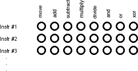
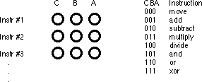
The CPU is a very complex piece of circuitry. Without going into too many details, let us just say that operations inside the CPU must be very carefully coordinated or the CPU will produce erroneous results. To ensure that all operations occur at just the right moment, the 80x86 CPUs use an alternating signal called the system clock.

2.1 The System Clock

At the most basic level, the system clock handles all synchronization within a computer system. The system clock is an electrical signal on the control bus which alternates between zero and one at a periodic rate:

CPUs are a good example of a complex synchronous logic system (see the previous chapter). The system clock gates many of the logic gates that make up the CPU allowing them to operate in a synchronized fashion.

The frequency with which the system clock alternates between zero and one is the system clock frequency. The time it takes for the system clock to switch from zero to one and back to zero is the clock period. One full period is also called a clock cycle. On most modern systems, the system clock switches between zero and one at rates exceeding several million times per second. The clock frequency is simply the number of clock cycles which occur each second. A typical 80486 chip runs at speeds of 66million cycles per second. 'Hertz' (Hz) is the technical term meaning one cycle per second. Therefore, the aforementioned 80486 chip runs at 66 million hertz, or 66 megahertz (MHz). Typical frequencies for 80x86 parts range from 5 MHz up to 200 MHz and beyond. Note that one clock period (the amount of time for one complete clock cycle) is the reciprocal of the clock frequency. For example, a 1 MHz clock would have a clock period of one microsecond (1/1,000,000th of a second). Likewise, a 10 MHz clock would have a clock period of 100 nanoseconds (100 billionths of a second). A CPU running at 50 MHz would have a clock period of 20 nanoseconds. Note that we usually express clock periods in millionths or billionths of a second.

To ensure synchronization, most CPUs start an operation on either the falling edge (when the clock goes from one to zero) or the rising edge (when the clock goes from zero to one). The system clock spends most of its time at either zero or one and very little time switching between the two. Therefore clock edge is the perfect synchronization point.

Since all CPU operations are synchronized around the clock, the CPU cannot perform tasks any faster than the clock. However, just because a CPU is running at some clock frequency doesn't mean that it is executing that many operations each second. Many operations take multiple clock cycles to complete so the CPU often performs operations at a significantly lower rate.

2.2 Memory Access and the System Clock

Memory access is probably the most common CPU activity. Memory access is definitely an operation synchronized around the system clock. That is, reading a value from memory or writing a value to memory occurs no more often than once every clock cycle. Indeed, on many 80x86 processors, it takes several clock cycles to access a memory location. The memory access time is the number of clock cycles the system requires to access a memory location; this is an important value since longer memory access times result in lower performance.

Different 80x86 processors have different memory access times ranging from one to four clock cycles. For example, the 8088 and 8086 CPUs require four clock cycles to access memory; the 80486 requires only one. Therefore, the 80486 will execute programs which access memory faster than an 8086, even when running at the same clock frequency.

Memory access time is the amount of time between a memory operation request (read or write) and the time the memory operation completes. On a 5 MHz 8088/8086 CPU the memory access time is roughly 800 ns (nanoseconds). On a 50 MHz 80486, the memory access time is slightly less than 20 ns. Note that the memory access time for the 80486 is 40 times faster than the 8088/8086. This is because the 80486's clock frequency is ten times faster and it uses one-fourth the clock cycles to access memory.

When reading from memory, the memory access time is the amount of time from the point that the CPU places an address on the address bus and the CPU takes the data off the data bus. On an 80486 CPU with a one cycle memory access time, a read looks something like shown below:

Writing data to memory is similar to:


Note that the CPU doesn't wait for memory. The access time is specified by the clock frequency. If the memory subsystem doesn't work fast enough, the CPU will read garbage data on a memory read operation and will not properly store the data on a memory write operation. This will surely cause the system to fail.

Memory devices have various ratings, but the two major ones are capacity and speed (access time). Typical dynamic RAM (random access memory) devices have capacities of four (or more) megabytes and speeds of 50-100 ns. You can buy bigger or faster devices, but they are much more expensive. A typical 33 MHz 80486 system uses 70 ns memory devices.

Wait just a second here! At 33 MHz the clock period is roughly 33 ns. How can a system designer get away with using 70 ns memory? The answer is wait states.

2.3 Wait States

A wait state is nothing more than an extra clock cycle to give some device time to complete an operation. For example, a 50 MHz 80486 system has a 20 ns clock period. This implies that you need 20 ns memory. In fact, the situation is worse than this. In most computer systems there is additional circuitry between the CPU and memory: decoding and buffering logic. This additional circuitry introduces additional delays into the system:

In this diagram, the system loses 10ns to buffering and decoding. So if the CPU needs the data back in 20 ns, the memory must respond in less than 10 ns.

You can actually buy 10ns memory. However, it is very expensive, bulky, consumes a lot of power, and generates a lot of heat. These are bad attributes. Supercomputers use this type of memory. However, supercomputers also cost millions of dollars, take up entire rooms, require special cooling, and have giant power supplies. Not the kind of stuff you want sitting on your desk.

If cost-effective memory won't work with a fast processor, how do companies manage to sell fast PCs? One part of the answer is the wait state. For example, if you have a 20 MHz processor with a memory cycle time of 50 ns and you lose 10 ns to buffering and decoding, you'll need 40 ns memory. What if you can only afford 80 ns memory in a 20 MHz system? Adding a wait state to extend the memory cycle to 100 ns (two clock cycles) will solve this problem. Subtracting 10ns for the decoding and buffering leaves 90 ns. Therefore, 80 ns memory will respond well before the CPU requires the data.

Almost every general purpose CPU in existence provides a signal on the control bus to allow the insertion of wait states. Generally, the decoding circuitry asserts this line to delay one additional clock period, if necessary. This gives the memory sufficient access time, and the system works properly

Sometimes a single wait state is not sufficient. Consider the 80486 running at 50 MHz. The normal memory cycle time is less than 20 ns. Therefore, less than 10 ns are available after subtracting decoding and buffering time. If you are using 60 ns memory in the system, adding a single wait state will not do the trick. Each wait state gives you 20 ns, so with a single wait state you would need 30 ns memory. To work with 60 ns memory you would need to add three wait states (zero wait states = 10 ns, one wait state = 30 ns, two wait states = 50 ns, and three wait states = 70 ns).

Needless to say, from the system performance point of view, wait states are not a good thing. While the CPU is waiting for data from memory it cannot operate on that data. Adding a single wait state to a memory cycle on an 80486 CPU doubles the amount of time required to access the data. This, in turn, halves the speed of the memory access. Running with a wait state on every memory access is almost like cutting the processor clock frequency in half. You're going to get a lot less work done in the same amount of time.

You've probably seen the ads. '80386DX, 33 MHz, 8 megabytes 0 wait state RAM only $1,000!' If you look closely at the specs you'll notice that the manufacturer is using 80 ns memory. How can they build systems which run at 33 MHz and have zero wait states? Easy. They lie.

There is no way an 80386 can run at 33 MHz, executing an arbitrary program, without ever inserting a wait state. It is flat out impossible. However, it is quite possible to design a memory subsystem which under certain, special, circumstances manages to operate without wait states part of the time. Most marketing types figure if their system ever operates at zero wait states, they can make that claim in their literature. Indeed, most marketing types have no idea what a wait state is other than it's bad and having zero wait states is something to brag about.

However, we're not doomed to slow execution because of added wait states. There are several tricks hardware designers can play to achieve zero wait states most of the time. The most common of these is the use of cache (pronounced 'cash') memory.

3 The Control Unit and Instruction Sets

A fair question to ask at this point is 'How exactly does a CPU perform assigned chores?' This is accomplished by giving the CPU a fixed set of commands, or instructions, to work on. Keep in mind that CPU designers construct these processors using logic gates to execute these instructions. To keep the number of logic gates to a reasonably small set (tens or hundreds of thousands), CPU designers must necessarily restrict the number and complexity of the commands the CPU recognizes. This small set of commands is the CPU's instruction set.

Programs in early (pre-Von Neumann) computer systems were often 'hard-wired' into the circuitry. That is, the computer's wiring determined what problem the computer would solve. One had to rewire the circuitry in order to change the program. A very difficult task. The next advance in computer design was the programmable computer system, one that allowed a computer programmer to easily 'rewire' the computer system using a sequence of sockets and plug wires. A computer program consisted of a set of rows of holes (sockets), each row representing one operation during the execution of the program. The programmer could select one of several instructions by plugging a wire into the particular socket for the desired instruction:

Of course, a major difficulty with this scheme is that the number of possible instructions is severely limited by the number of sockets one could physically place on each row. However, CPU designers quickly discovered that with a small amount of additional logic circuitry, they could reduce the number of sockets required from n holes for n instructions to lg(n) [log base 2] holes for n instructions. They did this by assigning a numeric code to each instruction and then encode that instruction as a binary number using lg(n) holes:

This addition requires eight logic functions to decode the A, B, and C bits from the patch panel, but the extra circuitry is well worth the cost because it reduces the number of sockets that must be repeated for each instruction.

Of course, many CPU instructions are not stand-alone. For example, the
move instruction is a command that moves data from one location in the computer to another (e.g., from one register to another). Therefore, the move instruction requires two operands: a source operand and a destination operand. The CPU's designer usually encodes these source and destination operands as part of the machine instruction, certain sockets correspond to the source operand and certain sockets correspond to the destination operand. The figure below shows one possible combination of sockets to handle this. The move instruction would move data from the source register to the destination register, the add instruction would add the value of the source register to the destination register, etc.
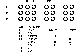
One of the primary advances in computer design that the VNA provides is the concept of a stored program. One big problem with the patch panel programming method is that the number of program steps (machine instructions) is limited by the number of rows of sockets available on the machine. John Von Neumann and others recognized a relationship between the sockets on the patch panel and bits in memory; they figured they could store the binary equivalents of a machine program in main memory and fetch each program from memory, load it into a special decoding register that connected directly to the instruction decoding circuitry of the CPU.

The trick, of course, was to add yet more circuitry to the CPU. This circuitry, the control unit (CU), fetches instruction codes (also known as operation codes or opcodes) from memory and moves them to the instruction decoding register. The control unit contains a special registers, the instruction pointer that contains the address of an executable instruction. The control unit fetches this instruction's code from memory and places it in the decoding register for execution. After executing the instruction, the control unit increments the instruction pointer and fetches the next instruction from memory for execution, and so on.

When designing an instruction set, the CPU's designers generally choose opcodes that are a multiple of eight bits long so the CPU can easily fetch complete instructions from memory. The goal of the CPU's designer is to assign an appropriate number of bits to the instruction class field (move, add, subtract, etc.) and to the operand fields. Choosing more bits for the instruction field lets you have more instructions, choosing additional bits for the operand fields lets you select a larger number of operands (e.g., memory locations or registers). There are additional complications. Some instructions have only one operand or, perhaps, they don't have any operands at all. Rather than waste the bits associated with these fields, the CPU designers often reuse these fields to encode additional opcodes, once again with some additional circuitry. The Intel 80x86 CPU family takes this to an extreme with instructions ranging from one to about ten bytes long. Since this is a little too difficult to deal with at this early stage, the x86 CPUs will use a different, much simpler, encoding scheme.

2 Encoding actual instructions

Although we could arbitrarily assign opcodes to each of the instructions for our processor, keep in mind that a real CPU uses logic circuitry to decode the opcodes and act appropriately on them. A typical CPU opcode uses a certain number of bits in the opcode to denote the instruction class (e.g., mov, add, sub), and a certain number of bits to encode each of the operands. Some systems (e.g., CISC, or Complex Instruction Set Computers) encode these fields in a very complex fashion producing very compact instructions. Other systems (e.g., RISC, or Reduced Instruction Set Computers) encode the opcodes in a very simple fashion even if it means wasting some bits in the opcode or limiting the number of operations. The Intel 80x86 family is definitely CISC and has one of the most complex opcode decoding schemes ever devised. The whole purpose for the hypothetical x86 processors is to present the concept of instruction encoding without the attendant complexity of the 80x86 family, while still demonstrating CISC encoding.

The didactic processor uses the following instruction format:

6 7 8 9 10 12 13 15

COP

d

MOD

REG

RM

COP the opcode that uniquely identifies the instruction (e.g. 0000000 means MOV, 0000010 means PUSH, etc.)

d the direction bit that specifies the destination of the result. The two operands of the instruction are indicated by the REG and RM fields of the instruction. If d=0 then the destination of the result is RM; if d=1 then the destination of the result is REG.

MOD - in conjunction with RM specifies one of the operands (e.g. MOD = 00 and RM = 100 indicates that the address of the operand is stored in register XA).

REG - specifies the other operand, in case this is a general-purpose register (e.g. REG = 000 indicates that the operand is stored in register RA).

RM - in conjunction with MOD specifies one of the operands.

Lets consider the following example:

MOV RC, [BA+XA]

The opcode for instruction MOV is 0000000.

One of the operands is specified using indirect addressing by register sum. The two registers are respectively BA and XA. The proper combination for that is: MOD = 00 and RM = 000.

The other operand is register RC, thus REG is 001.

The result will be register RC (specified by REG), thus d = 1.

Consequently, the instruction will be encoded as:

Please refer to the Computer Architecture course on how the actual values were selected. Also, please note that this is only a part of the story and more things are still to come. For example we havent discussed what happens with immediate addressing (MOV RA,2) or direct addressing (MOV RA,[2]). All of these are included in the course.


DISTRIBUIE DOCUMENTUL


Politica de confidentialitate | Termeni si conditii de utilizare


DISTRIBUIE DOCUMENTUL

Comentarii


Vizualizari: 1086
Importanta: rank

Comenteaza documentul:

Te rugam sa te autentifici sau sa iti faci cont pentru a putea comenta

Creaza cont nou

Termeni si conditii de utilizare | Contact
© SCRIGROUP 2024 . All rights reserved