| CATEGORII DOCUMENTE |
| Bulgara | Ceha slovaca | Croata | Engleza | Estona | Finlandeza | Franceza |
| Germana | Italiana | Letona | Lituaniana | Maghiara | Olandeza | Poloneza |
| Sarba | Slovena | Spaniola | Suedeza | Turca | Ucraineana |
DOCUMENTE SIMILARE |
|
TERMENI importanti pentru acest document |
|
Electronics Laboratory - Diodes
1. Measure td.
We have taken the following hardcopy and measured td using the cursors;
we can see that td. = 8.8 ns = 8.8 * 10![]() s. 10X attenuation factor was used for the probes
since such small delay times imply very high frequencies.
s. 10X attenuation factor was used for the probes
since such small delay times imply very high frequencies.

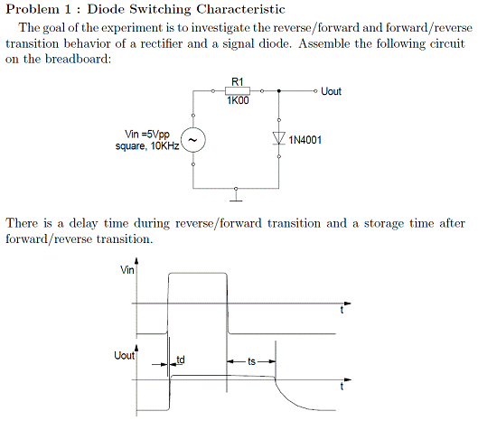
2. Measure ts.
We have taken the following hardcopy and measured ts using the cursors ; we can see that td. = 4.68 ![]() s = 4.68 * 10
s = 4.68 * 10![]() s.
s.
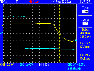
3. Now replace the 1N4001 rectifier diode by a 1N4148 signal diode and repeat the ts measurement.
We have taken the following hardcopy and measured ts using the cursors ; we can see that td. = 14.2 ns = 14.2 * 10![]() s.
s.
1. Give a comment about the delay time!
A diode can be used as a switch:
Under forward-bias, a large amount of current can flow through the diode, but with a relatively small voltage across the diode – a short circuit.
Under reverse-bias, almost no current flows through the diode, but a voltage potential still appears – an open circuit.
While a diode is not a true switch, it is often used in switching applications since the switching times attainable with diodes is considerably smaller than with mechanical switches
The delay time is defined as the time between the reverse and forward transition.
In this case, this time is considerably small (8.8 nanoseconds) which actually means that the diode starts conducting very quickly. The applied voltage supplies enough energy to the free charges to overcome the barrier, and thus the carriers can cross the junction and the depletion region is shrinking. (Current is flowing – negative charges in the p-side go to the positive applied voltage and positive charges in the n-side go to the negative applied voltage).
2. Compare the two storage times. What is the reason why the diodes need that long time to switch off?
First of all, at the switch time, the current reverses and stays at a constant level for a period of time called the storage time, ts. During this time the diode acts essentially as a short circuit. Then the current decreases to the reverse leakage current value.
We observe that the storage time for the 1N4148 model is significantly
smaller than for the 1N4001 model (8.8 nanoseconds compared to 4.68 microseconds,
so ![]() 531 times smaller).
531 times smaller).
When the input square voltage (v (t)) is positive, the diode is forward biased; when v (t) is negative, the diode is reverse biased. With v (t) constant at +2.5 V, the diode is forward biased, and almost all of 2.5V will appear across the resistor if V0 (turn-on voltage of the diode) is much smaller than 2.5 V. Thus, the steady-state current i = If ≈ 2.5/1000A = 2.5 mA flows. When v (t) is switched to -2.5V, the diode is now reverse biased. One would expect that almost no current would flow. However, the stored minority carriers and excess majority carriers in the diode cannot be removed instantaneously. The excess majority carriers flow out of the system while the stored minority carriers flow back across the junction or recombine. Since the excess carriers (both minority and majority) are given by the relation Q = If ·tp in a p -n junction, to remove these, a reverse current Ir must flow for some finite time. Thus, an initial reverse current i = –Ir ≈ –2.5/1000A = - 0.25 A must flow. As the charge is redistributed, more and more of 2.5 V will appear across the diode, since the diode is reverse-biased. This will decrease the voltage across the resistor, and thereby the current becomes smaller as time proceeds.
The storage delay time can be defined also as the time it takes for the stored charge to become zero while the redistribution of charge takes place when switching from +2.5V to –2.5V. This delay time is an important factor in rating diodes for switching applications. It is desirable to have ts small compared to the switching times necessary in a specific application. This storage delay time is a direct function of the carrier lifetime.
3. What are the consequences for using these diodes in different applications ? Think of the AM demodulation experiment when using several 100 KHZ!
The reverse recovery time values for p-n junction diodes are in the
range of a few hundred nanoseconds to a
couple of milliseconds for the General Purpose Rectifiers ( looking at the table below ,for the 1N4001
diode , we observe a value of 2![]() which is basically
close to our measured value : 4.68
which is basically
close to our measured value : 4.68![]() ).
).
When the diode is used as a rectifier for 60 Hz voltage in a power supply, the reverse recovery time won’t be so relevant within the above mentioned range.
But when the diode is used as a switch in a circuit with a 100 KHz frequency voltage supply, then 2 milliseconds represent a critical part of the conduction cycle and as a result, the signal will suffer severe distortion. As another result, the diode will dissipate a lot of energy and the efficiency can dramatically suffer in the case of DC-DC converters.
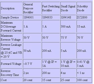
Table 1.
![]()
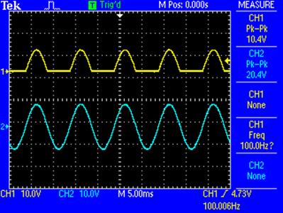
Fig 2.1.a

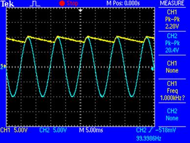
Fig 2.1.b
![]()
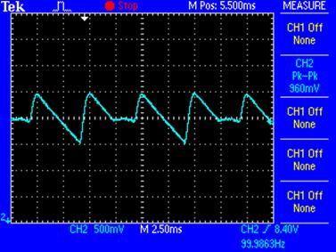
Fig. 2.2.a

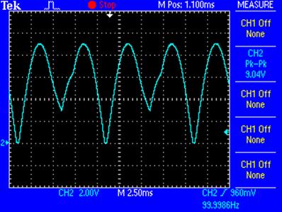
Fig. 2.2.b
2.1

![]()
![]()
![]()
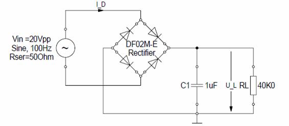
Fig. 2.1
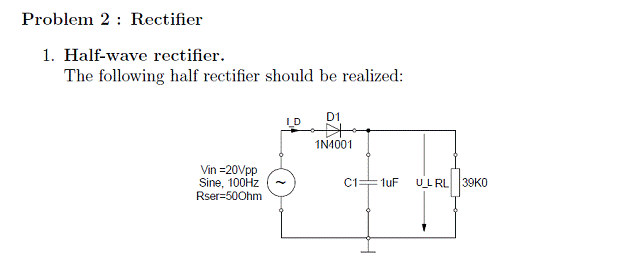
The building blocks of a DC power supply are:
A) Power Supply: this component provides a potential difference to power the circuit. This voltage difference, however, changes with time from Vmax to –Vmax in the form of a sine wave.
What is desired is a voltage difference which is as stable as possible over time. Therefore, the next step would be to revert the negative values of the voltage to positive. This is accomplished by the building block B:
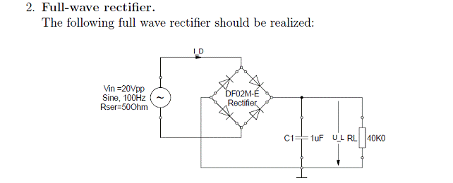
B) This building block redirects the current flow through two different paths depending of the polarity of the voltage in order to achieve only positive values of this difference. The full wave rectifier provides a better power usage (50% more) than half wave rectifier and also a smoother output after the next block, C:
C) The purpose of adding a capacitor is to restrict the voltage from falling when the power supply voltage is decreasing. This is done by charging the capacitor (at the same pace with the voltage rise) and discharging it with a time constant τ=R·C.

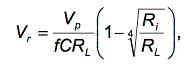
For calculating the ripple value, we will use the formula in the handout :
(I) Calculating Vrh ( half-wave rectifier )
Vp = 10.02 V, f = 100 Hz, C = 1![]() F, Ri = 50
F, Ri = 50![]() and RL
= 40 K
and RL
= 40 K![]()
So Vr = ![]() 2.487 * 0.812 V= 2.019 V
2.487 * 0.812 V= 2.019 V
(II) Calculating Vrf ( full-wave rectifier )
For full-wave rectifier we must take half the value from the half-wave rectifier:
Vp = 5.01 V, f = 100 Hz, C = 1![]() F, Ri = 50
F, Ri = 50![]() and RL
= 39000
and RL
= 39000 ![]()
So Vr = ![]() 1.284 * 0.811V = 1.041V
1.284 * 0.811V = 1.041V
|
Output ripple Vr |
Calculated value [V] |
Oscilloscope measured value [V] |
Spice measured value [V] |
|
Vrh( half-wave) |
2.016 |
2.200 |
1.897 |
|
Vrf(full-wave) |
1.041 |
0.960 |
0.838 |
Taking as reference the calculated value, we obtain the following set of errors:
|
Error(%) |
Vrh |
Vrf |
|
Oscilloscope value |
9.12 |
5.90 |
|
Spice value |
14.23 |
19.50 |
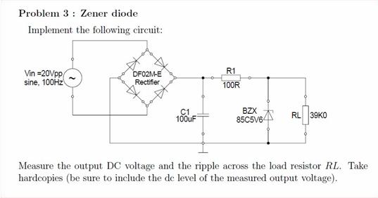
Fig. 3.1
The dc value is given by the CH1 mean value in the above hardcopy Fig. 3.1
![]()
The ripple voltage is given by the CH1 VPP value in the above hardcopy Fig. 3.1.
![]()
Since the voltage after the rectifier block still change, we will first compute the upper limit of the current through the diode. Therefore we should consider the following:
![]() (Before 100Ω resistor)
(Before 100Ω resistor)
![]()
![]()
This voltage drop over the R1 resistor is caused by the current flowing through Zener diode:
![]()
The max value of the current through the diode is 47mA
![]()
![]()
![]()
=>![]()
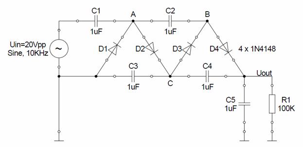
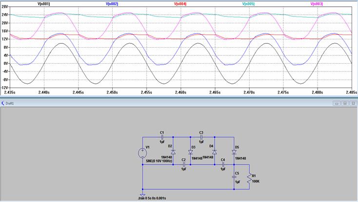
PROBLEM 4 – Voltage Multiplier
The following circuit was assembled on the breadboard:
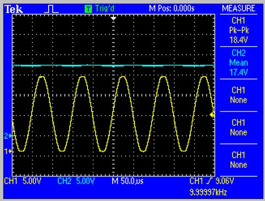
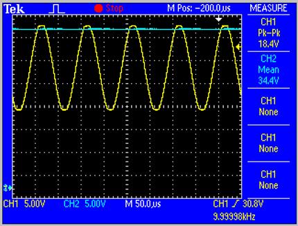
1. Using the oscilloscope, the voltages at points ‘A’ and ‘C’ were measured. The hardcopy obtained is showed below(CH 1 was connected to ‘A’ and CH 2 was connected to point ‘C’):
2. Using the oscilloscope, the voltages at points ‘B’ and ‘Uout’ were measured. The hardcopy obtained is showed below(CH 1 was connected to ‘B’ and CH 2 was connected to ‘Uout’):
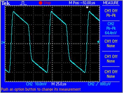
3. Using the oscilloscope, the ripple voltage was measured at ‘Uout’. Hardcopy below:
1.
The circuit consists of a series of positive clampers
and half-wave voltage rectifiers and has the overall function of voltage
multiplier. It takes the input AC voltage and converts it to a DC (with a
certain ripple) voltage of higher value.
The section between the input and point A acts as a positive clamper, effectively adding a DC voltage level equal to the input voltage to the output signal. The section between point A and point C acts as a half wave voltage rectifier, thus having a DC voltage at its output. The next sections continue to raise the voltage, in the ideal case, doubling the input for each series of 1 clamper and 1 rectifier.

2. At the negative peak of the input voltage, the right plate of C1 capacitor is charged through diode D1 to 0V (connected to ground), while the left plate is charged to -10V.Thus, the potential difference ‘held’ by the capacitor is 10V. Next, at the positive peak, the potential across the capacitor adds with the potential of the source, thus charging C3 to 20V, because the left plate of C3 is connected to ground (0V), while the right plate is connected to the right plate of C1 through D2. At the next negative input peak, the potential of C1 drops to 0V and C2 is charged through D3 to 20V. At the next positive peak, the potential across C1 rises to 20V, also charging C4 to 20V. The result at the output will be the sum of the voltages across C2 and C4, so 40V. Thus, each pair of clamper and rectifier produces as output a DC voltage with 2 times the value of the input peak voltage, effectively acting as a voltage doubler.
Ideally, the output voltage would be 40V. However, we need to subtract 4·cut in voltage of the 1N4148 diode, which is about 0.65V. We also need to subtract the voltage drop across the connecting wires and connections which have a small, but non-zero resistance. Also, there is a voltage drop across each capacitor which has an impedance proportional to its capacitance and the frequency of the input: ZC = 1/(j·Ѡ·C).
The function of the circuit can be visualized using the diagram below obtained by simulating the circuit in PSpice.
The 10V peak amplitude AC sine signal V(n001) is shifted up by its input peak voltage (minus the cut in voltage of the diode) using the clamper. The result V(n002) is passed through the rectifier circuit to obtain a DC voltage of about 18V = V(n004). Then, this voltage is clamped to V(n003), which is a sine wave obtained by shifting V(n002) by its peak to peak voltage over V(n004), effectively doubling it to 36V. Finally, using the second half-wave rectifier, the final voltage V(n005) is obtained, which is about 37V.
Each time a sine signal is passed through a half wave rectifier, the capacitor is charged during the rising voltage part and, assuming the time constant (τ = R·C) is considerably higher than the signal period = 1/f, the decaying exponential shape of the voltage can be approximated to a straight line connecting the peak voltage points of the sine wave, thus having a DC voltage as output.
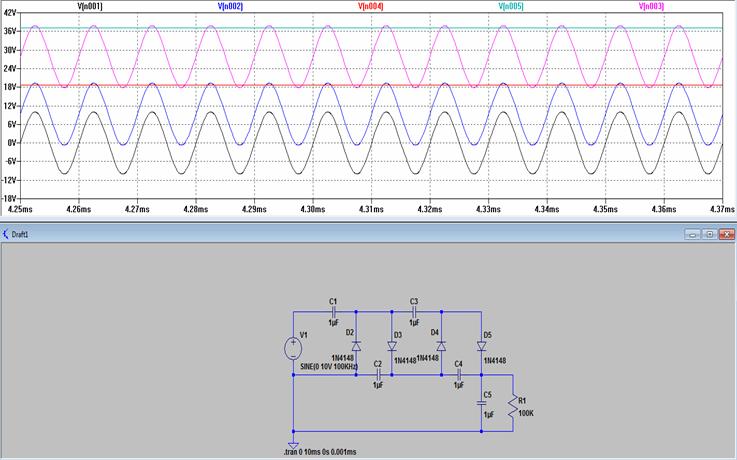
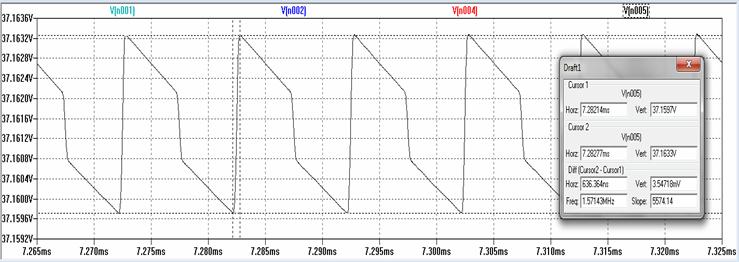
3. The input and output voltages for the PSpice simulation were measured using cursors.
For the PSpice simulation: Vin = 9.987V and Vin = 37.142V. The multiplication factor is thus
Vout/Vin = 3.72
Theoretically, neglecting the voltage drops across diodes, wires and capacitors, the input voltage should be Vin = 10V and the output voltage should be Vout = 40V. The multiplication factor is thus
Vout/Vin = 4
For the measured values with the oscilloscope, we have: Vout = 34.4V. Taking Vin = 10V, we get:
Vout/Vin = 3.44
For the measured values with the multimeter, we have: Vout = 35.19V. Taking Vin = 10V, we get:
Vout/Vin = 3.519
The difference between the theoretical and the measured values comes mainly from the voltage drops across the 4 1N4148 diodes (4·Vcut in = 4·0.7V = 2.8V). There are also voltage drops across the connecting wires and electrical connections and also voltage drops across the capacitors, which have an impedance of 1/(j·Ѡ·C) and also a certain parasitic capacitance.
Although the PSpice simulation takes into account the forward voltage of the diodes, it does not consider the voltage drop across wires and capacitors.
The difference between the values measured with the oscilloscope and multimeter comes from the internal resistance of the 2 devices, which differs. Specifically, the impedance of the probes is higher than that of the multimeter connectors, thus the voltage drop over the probes is higher than that over the multimeter connectors, resulting is a higher value of the output measured with the multimeter (35.19V) than that with the oscilloscope: 34.4V
4. Although the output voltage can be very large – more than thousands of volts, the individual components do not need to be able to withstand this high voltage. Each component only needs to withstand the voltage difference directly across its own terminals and of the components immediately adjacent to it. In our case this difference is twice the input voltage, about 20V. So, every component needs to withstand only 20V, not 40V. If the circuit had, for example 10 stages, instead of 2, the output voltage would ideally be about 10 KV, but each component would only need to withstand a much smaller voltage value.
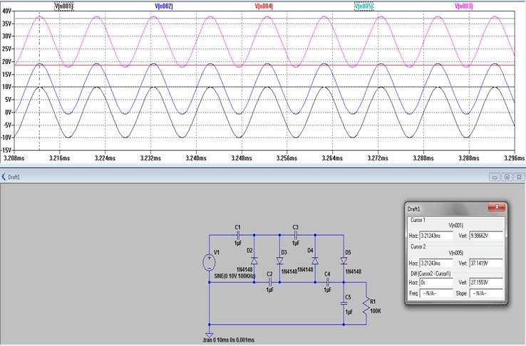
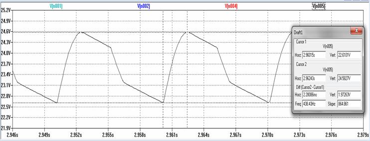
5. If the input frequency is reduced from 10KHz to 100Hz, the impedance of each resistor increases dramatically 100 times, following ZC = 1/(j·Ѡ·C). Thus, the voltage drop over the capacitors, which was very small initially, increases to a few volts, decreasing the output voltage as it can be seen in the diagram below obtained by simulating the circuit in PSpice. Also, by reducing the frequency, the input signal period increases 100 times, while the time constant τ = R·C remains constant, thus the voltage across the capacitor has time to drop, increasing the ripple voltage.
As it can be seen from the graph above, the output voltage dropped from 37.1V to 24V.
The ripple voltage increased dramatically from 3.547mV to 1.973V.
References:
David J. Comer, Donald T. Comer, Fundamentals of Electronic Circuit Design,
John Wiley & Sons
Adel S.
Sedra, Kennth C. Smith, Microelectronic Circuits,
Publishing, 3rd ed., ISBN:0-03-051648-X, 1991.
Electronics Lab Handout
|
Politica de confidentialitate | Termeni si conditii de utilizare |

Vizualizari: 500
Importanta: ![]()
Termeni si conditii de utilizare | Contact
© SCRIGROUP 2025 . All rights reserved