| CATEGORII DOCUMENTE |
| Bulgara | Ceha slovaca | Croata | Engleza | Estona | Finlandeza | Franceza |
| Germana | Italiana | Letona | Lituaniana | Maghiara | Olandeza | Poloneza |
| Sarba | Slovena | Spaniola | Suedeza | Turca | Ucraineana |
The term 'combinational' comes to us from mathematics. In mathematics a combination is an unordered set, which is a formal way to say that nobody cares which order the items came in. With combinational logic, the circuit produces the same output regardless of the order the inputs are changed. There are circuits which depend on the when the inputs change, these circuits are called sequential logic. Practical circuits will have a mix of combinational and sequential logic, with sequential logic making sure everything happens in order and combinational logic performing functions like arithmetic, logic, or conversion.
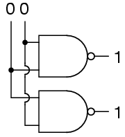
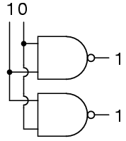
Each logic gate discussed previously is a combinational logic function. Lets follow how two NAND gate works if we provide them inputs in different orders.
We begin with both inputs being 0.
We then set one input high.
We then set the other input high.
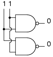
So NAND gates do not care about the order of the inputs, and you will find the same true of all the other gates covered up to this point (AND, XOR, OR, NOR, XNOR, and NOT).
As a first example of useful combinational circuit, we build a device that can add two binary digits together. We can quickly calculate what the answers should be:
0 + 1 = 1 1 + 0 = 1 1 + 1 = 102So we will need two inputs (a and b) and two outputs. The low order output will be called Σ because it represents the sum, and the high order output will be called Cout because it represents the carry out.
The truth table is:
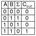
Simplifying boolean equations will produce
the same circuit shown below, but start by looking at the results. The Σ
column is our familiar XOR gate, while the Cout column is the AND
gate. 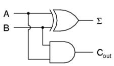
The half-adder is extremely useful until you want to add more that one binary digit quantities. The slow way to develop a two binary digit adders would be to make a truth table and reduce it. Then when you decide to make a three binary digit adder, do it again. And so on The circuits would be fast, but development time would be slow.
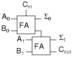
The three binary digit adder needs three inputs; a, b, and the carry from the previous sum, and we can use our two-input adder to build a three input adder.
Σ is the easy part. Normal arithmetic tells us that if Σ = a + b + Cin and Σ1 = a + b, then Σ = Σ1 + Cin.
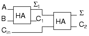
What do we do with C1 and C2? Let's look at three input sums and quickly calculate:
Cin + a + b = ?In order to calculate the high order bit, notice that it is 1 in both cases when a + b produces a C1. Also, the high order bit is 1 when a + b produces a Σ1 and Cin is a 1. So, we will have a carry when C1 OR (Σ1 AND Cin). The complete three input adder is:
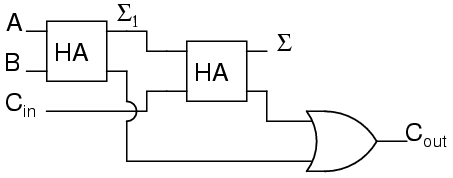
For some designs, being able to eliminate one or more types of gates can be important, and you can replace the final OR gate with an XOR gate without changing the results.
We can now connect two adders to add 2 bit quantities.
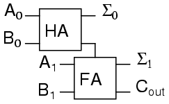
A0 is the low order bit of A, A1 is the high order bit of A, B0 is the low order bit of B, B1 is the high order bit of B, Σ0is the low order bit of the sum, Σ1 is the high order bit of the sum, and Cout is the Carry.
A two binary digit adder would never be made this way. Instead the lowest order bits would also go through a full adder too.
There are several reasons for this, one being that we can then allow a circuit to determine whether the lowest order carry should be included in the sum. This allows for the chaining of even larger sums. These full adders can also can be expanded to any number of bits we choose. As an example, here's how to do an 8 bit adder.
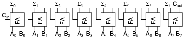
This is the same result as using the two 2-bit adders to make a 4-bit adder and then using two 4-bit adders to make an 8-bit adder.
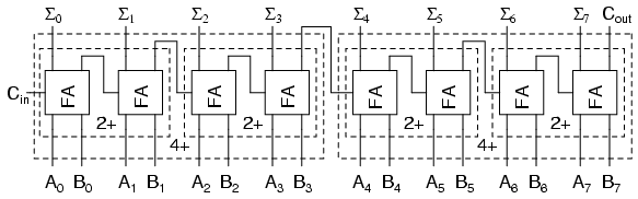
Each '2+' is a 2-bit adder and made of two full adders. Each '4+' is a 4-bit adder and made of two 2-bit adders. And the result of two 4-bit adders is the same 8-bit adder we used full adders to build.
For any large combinational circuit there are generally two approaches to design: you can take simpler circuits and replicate them; or you can design the complex circuit as a complete device. Using simpler circuits to build complex circuits allows a you to spend less time designing but then requires more time for signals to propagate through the transistors. The 8-bit adder design above has to wait for all the Cxout signals to move from A0 + B0 up to the inputs of Σ7.
When designing for systems that have a maximum allowed response time to provide the final result, you can begin by using simpler circuits and then attempt to replace portions of the circuit that are too slow.
A decoder is a circuit that changes a code into a set of signals. It is called a decoder because it does the reverse of encoding, but we will begin our study of encoders and decoders with decoders because they are simpler to design.
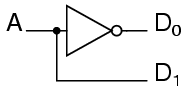
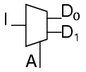
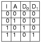
A common type of decoder is the line decoder which takes an n-digit binary number and decodes it into 2n data lines. The simplest is the 1-to-2 line decoder. The truth table is
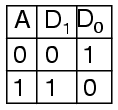
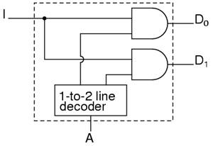
A is the address and D is the dataline. D0 is NOT A and D1 is A. The circuit looks like
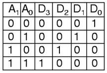
Only slightly more complex is the 2-to-4 line decoder. The truth table is
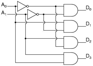
Developed into a circuit it looks like:
Larger line decoders can be designed in a similar fashion, but just like with the binary adder there is a way to make larger decoders by combining smaller decoders.
An alternate circuit for the 2-to-4 line decoder is:
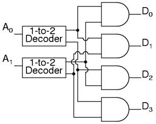
Replacing the 1-to-2 Decoders with their circuits will show that both circuits are equivalent. In a similar fashion a 3-to-8 line decoder can be made from a 1-to-2 line decoder and a 2-to-4 line decoder, and a 4-to-16 line decoder can be made from two 2-to-4 line decoders.
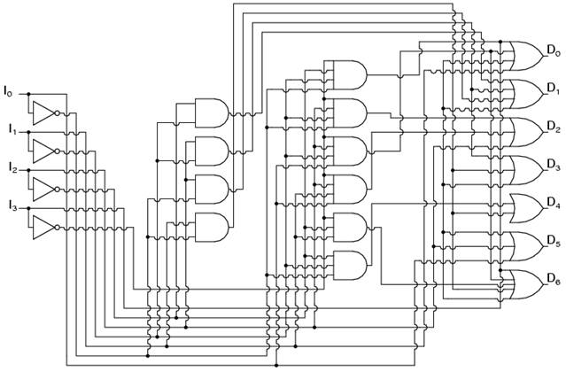
A typical application of this circuit is to select among multiple devices. A circuit needing to select among sixteen devices could have sixteen control lines to select which device should 'listen'. With a decoder only four control lines are needed.
An encoder is a circuit that changes a set of signals into a code. We begin making a 2-to-1 line encoder truth table by reversing the 1-to-2 decoder truth table.

This truth table is a little short. A complete truth table would be
One question we need to answer is what to do with those other inputs? Do we ignore them? Do we have them generate an additional error output? In many circuits this problem is solved by adding sequential logic in order to know not just what input is active but also which order the inputs became active.
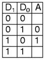
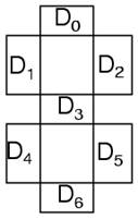
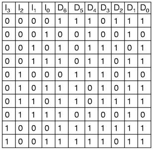
A more useful application of combinational encoder design is a binary to 7-segment encoder. The seven segments are given according:
The truth table is:
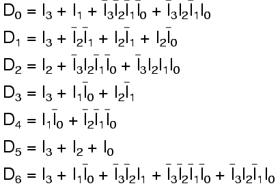
Deciding what to do with the remaining six entries of the truth table is easier with this circuit. This circuit should not be expected to encode an undefined combination of inputs, so we can leave them as 'don't care' when we design the circuit. The boolean equations are
and the circuit is
A demultiplexer, abbreviated DMUX, is a circuit that has one input and more outputs. It is used when a circuit wishes to send a signal to one of many devices. This description sounds similar to the description given for a decoder, but a decoder is used to select among many devices while a demultiplexer is used to send a signal among many devices.
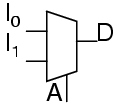
A demultiplexer is used often enough that it has its own schematic symbol
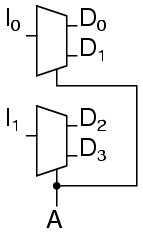
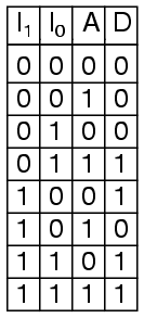
The truth table for a 1-to-2 demultiplexer is
Using our 1-to-2 decoder as part of the circuit, we can express this circuit easily
This circuit can be expanded two different ways. You can increase the number of signals that get transmitted, or you can increase the number of inputs that get passed through. To increase the number of inputs that get passed through just requires a larger line decoder. Increasing the number of signals that get transmitted is even easier.
As an example, a device that passes one set of two signals among four signals is a 'two-bit 1-to-2 demultiplexer'. Its circuit is
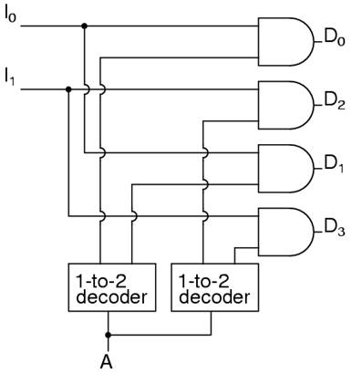
or by expressing the circuit as:
shows that it could be two one-bit 1-to-2 demultiplexers without changing its expected behavior.
A multiplexer, abbreviated MUX, is a device that has multiple inputs and one output.
The schematic symbol for multiplexers is
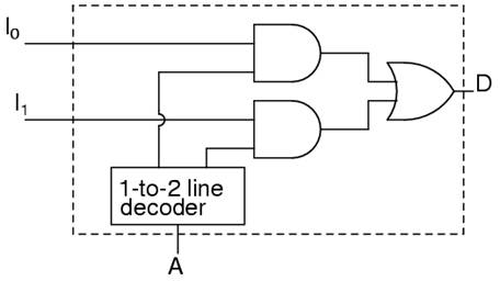
The truth table for a 2-to-1 multiplexer is
Using a 1-to-2 decoder as part of the circuit, we can express this circuit easily.
Multiplexers can also be expanded with the same naming conventions as demultiplexers.
That is the formal definition of a multiplexer. Important, sometimes, both demultiplexers and multiplexers have similar names, abbreviations, schematic symbols and circuits, so confusion is easy. The term multiplexer, and the abbreviation mux, are often used to also mean a demultiplexer, or a multiplexer and a demultiplexer working together. So when you hear about a multiplexer, it may mean something quite different.
|
Politica de confidentialitate | Termeni si conditii de utilizare |

Vizualizari: 1468
Importanta: ![]()
Termeni si conditii de utilizare | Contact
© SCRIGROUP 2025 . All rights reserved