| CATEGORII DOCUMENTE |
| Bulgara | Ceha slovaca | Croata | Engleza | Estona | Finlandeza | Franceza |
| Germana | Italiana | Letona | Lituaniana | Maghiara | Olandeza | Poloneza |
| Sarba | Slovena | Spaniola | Suedeza | Turca | Ucraineana |
Circuit 45 Astable latched
Function
Once triggered, LEDs will continue to flash until power is removed from the circuit or SW1 is opened. The rate at which LEDs flash is controlled by adjustment of VR1.
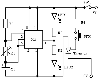
Circuit diagram
R1 = 1k ohm
R2 = 470 ohm
R3 = 470 ohm
R4 = 47k ohm
VR1 = 100k ohm
IC1 555 Timer
Thyristor = (TIC106D)
5mm Standard LEDs
Operation
Heart of the circuit is a 555-timer chip configured in ASTABLE MODE.
This means the output at pin 3 is constantly changing i.e. the output goes high (9V) for a specified time, and then low (0V) for a specified time before again switching high.
The transition from high to low and back to high is called a cycle and the number of cycles which occur in one second is called the frequency, measured in hertz (symbol Hz).
The frequency is controlled by the size of R1, VRI and C1.
Formula to calculate the frequency:-
![]()
With VR1 adjusted to its maximum value.
Frequency = 0.07Hz
The time taken to complete one cycle (known as the PERIOD symbol T), can be calculated from the formula.
![]()
T = 14.2 sec.
If R1 is made much smaller than VR1, (i.e. R1 is approximately one tenth VR1or less).
Then the time LED is lit will be the same as the time unlit, i.e. lit for 7.1 sec., unlit 7.1 sec.
This time can be made shorter by reducing the value of VR1.
Consider the output pin 3 (555 timer) is low, 0V, top LED in series with R2 is connected from the 9V rail to pin 3, therefore this LED is lit.
Bottom LED in series with R3 is connected to pin 3 (0V) to the bottom rail (0V), therefore this LED is unlit.
Consider now output (pin 3) goes high (9V). With 9V on the top rail and 9V on pin 3, there is no voltage drop across top LED, so it is unlit.
With 9V on pin 3 (ASTABLE) and 0V on the bottom rail bottom LED is therefore lit, thus both LEDs flash on and off alternately at a pre-determined rate.
Calculation of Voltage Dropper Resistors R3, and R2.
It is most important an LED must not have any more than 2V dropped across it. Also the current flowing through it should not exceed 20mA.
The LEDs are connected to the (9V) outputs of the ASTABLE circuit to 0V rail, and also from the 9V supply rail to the 0V output of pin 3 of the astable circuit.
Therefore 7V must be dropped across a resistor called a voltage dropper resistor. As the max current permissible through an LED is 20mA OHMS LAW can be used to calculate value of resistor.
R =7/0.20 ==350 ohms
It is not good practice to have components operating on their top limit, i.e. 20mA. Therefore make resistor larger, say 470 ohms.
This has the dual advantage of protecting the LED, and also drawing less current from the battery, thus prolonging its life at the expense of the LED being a little less bright.
With 0V applied to the gate of the thyristor, it is switched off, no current can flow from the anode to the cathode, so there is no path for the current required to operate the 555 timer to return to ground. Thus 555 circuit cannot operate.
Consider PTM switch is pressed.
9V now applied to the gate of the thyristor. Thyristor will pass current easily. Current can flow through the astable circuit, through thyristor, to the 0V rail, so LEDS will flash. Once switched on, it will continue to pass current even if the positive voltage is removed from the gate i.e. the circuit is latched.
If excess current is allowed to flow into the gate of the thyristor, it can cause damage.
It is for this reason that R4 is inserted to restrict the flow of current (use 47k ohm).
Consider now the overall circuit.
No current can flow through the 555-timer circuit as pin 1 is connected to the anode of the thyristor, and in the present state it is switched off. Thus LEDs are unlit.
If PTM switch is pressed, a positive voltage is applied to the gate of thyristor so it will switch on. There is now a path for the current from pin 1 (555) to flow to ground i.e. via the anode and cathode of the thyristor, thus timer circuit will switch on and LEDs will light.
|
Politica de confidentialitate | Termeni si conditii de utilizare |

Vizualizari: 959
Importanta: ![]()
Termeni si conditii de utilizare | Contact
© SCRIGROUP 2026 . All rights reserved