| CATEGORII DOCUMENTE |
| Bulgara | Ceha slovaca | Croata | Engleza | Estona | Finlandeza | Franceza |
| Germana | Italiana | Letona | Lituaniana | Maghiara | Olandeza | Poloneza |
| Sarba | Slovena | Spaniola | Suedeza | Turca | Ucraineana |
DOCUMENTE SIMILARE |
|
TERMENI importanti pentru acest document |
|
| : | |
The operational amplifier is the most useful single device in analog electronic circuitry. With only a few external components it can be made to perform a wide variety of analog signal processing tasks. Modern designs have been engineered with durability in mind as well: several 'op-amps' are manufactured that can sustain direct short-circuits on their outputs without damage.
One key to the usefulness of these little circuits is in the engineering principle of feedback, particularly negative feedback, which constitutes the foundation of almost all automatic control processes.
For ease of drawing complex circuit diagrams, electronic amplifiers are often symbolized by a simple triangle shape, where the internal components are not individually represented.
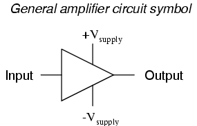
The +V and -V connections denote the positive and negative sides of the DC power supply, respectively. The input and output voltage connections are shown as single conductors, because it is assumed that all signal voltages are referenced to a common connection in the circuit called ground. Often (but not always!), one pole of the DC power supply, either positive or negative, is that ground reference point. A practical amplifier circuit (showing the input voltage source, load resistance, and power supply) is in the following figure presented:
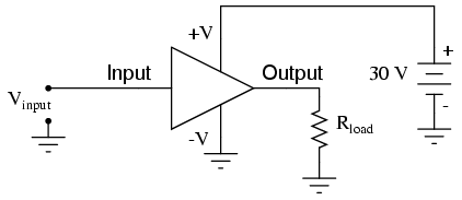
It can be easily understood the circuit's function: to take an input signal (Vin), amplify it, and drive a load resistance (Rload). To complete the above schematic, it would be good to specify the gains of that amplifier (AV, AI, AP) and the Q (bias) point for any needed mathematical analysis.
If it is necessary for an amplifier to be able to output true AC voltage (reversing polarity) to the load, a split DC power supply may be used, whereby the ground point is electrically 'centered' between +V and -V. Sometimes the split power supply configuration is referred to as a dual power supply.
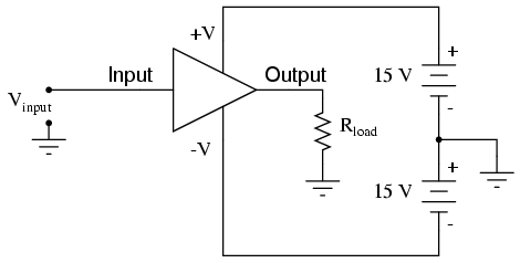
The amplifier is still being supplied with 30 volts overall, but with the split voltage DC power supply, the output voltage across the load resistor can now swing from a theoretical maximum of +15 volts to -15 volts, instead of +30 volts to 0 volts. This is an easy way to get true alternating current (AC) output from an amplifier without resorting to capacitive or inductive (transformer) coupling on the output.
One of the more complex amplifier types that is derived from OA is called differential amplifier. Unlike normal amplifiers, which amplify a single input signal (often called single-ended amplifiers), differential amplifiers amplify the voltage difference between two input signals. Using the simplified triangle amplifier symbol, a differential amplifier looks like this:
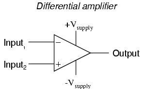
The two input leads can be seen on the left-hand side of the triangular amplifier symbol, the output lead on the right-hand side, and the +V and -V power supply leads on top and bottom. As with the other example, all voltages are referenced to the circuit's ground point. Notice that one input lead is marked with a (-) and the other is marked with a (+). Because a differential amplifier amplifies the difference in voltage between the two inputs, each input influences the output voltage in opposite ways. Consider the following table of input/output voltages for a differential amplifier with a voltage gain of 4:
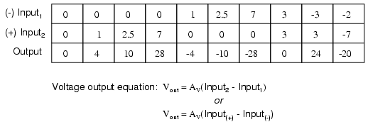
An increasingly positive voltage on the (+) input tends to drive the output voltage more positive, and an increasingly positive voltage on the (-) input tends to drive the output voltage more negative. Likewise, an increasingly negative voltage on the (+) input tends to drive the output negative as well, and an increasingly negative voltage on the (-) input does just the opposite. Because of this relationship between inputs and polarities, the (-) input is commonly referred to as the inverting input and the (+) as the noninverting input.
From the sign point of view, the OA works like a digital voltmeter:
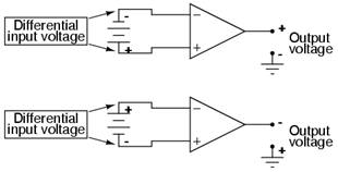
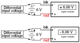
When the polarity of the differential voltage matches the markings for inverting and noninverting inputs, the output will be positive. When the polarity of the differential voltage clashes with the input markings, the output will be negative. This bears some similarity to the mathematical sign displayed by digital voltmeters based on input voltage polarity. The red test lead of the voltmeter (often called the 'positive' lead because of the color red's popular association with the positive side of a power supply in electronic wiring) is more positive than the black, the meter will display a positive voltage figure, and vice versa:
Just as a voltmeter will only display the voltage between its two test leads, an ideal differential amplifier only amplifies the potential difference between its two input connections, not the voltage between any one of those connections and ground. The output polarity of a differential amplifier, just like the signed indication of a digital voltmeter, depends on the relative polarities of the differential voltage between the two input connections.
If the input voltages to this amplifier represented mathematical quantities (as is the case within analog computer circuitry), or physical process measurements (as is the case within analog electronic instrumentation circuitry), the differential amplifier could be very useful. It could be used to compare two quantities to see which is greater (by the polarity of the output voltage), or to compare the difference between two quantities (such as the level of liquid in two tanks) and flag an alarm (based on the absolute value of the amplifier output) if the difference became too great. In basic automatic control circuitry, the quantity being controlled (called the process variable) is compared with a target value (called the setpoint), and decisions are made as to how to act based on the discrepancy between these two values. The first step in electronically controlling such a scheme is to amplify the difference between the process variable and the setpoint with a differential amplifier. In simple controller designs, the output of this differential amplifier can be directly utilized to drive the final control element (such as a valve) and keep the process reasonably close to setpoint.
CONCLUSIONS:
Long before of digital electronic technology, computers were built to electronically perform calculations by employing voltages and currents to represent numerical quantities. This was especially useful for the simulation of physical processes. A variable voltage, for instance, might represent velocity or force in a physical system. Through the use of resistive voltage dividers and voltage amplifiers, the mathematical operations of division and multiplication could be easily performed on these signals.
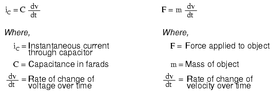
The reactive properties of capacitors and inductors lend themselves well to the simulation of variables related by calculus functions. Remember how the current through a capacitor was a function of the voltage's rate of change, and how that rate of change was designated in calculus as the derivative? Well, if voltage across a capacitor were made to represent the velocity of an object, the current through the capacitor would represent the force required to accelerate or decelerate that object, the capacitor's capacitance representing the object's mass:
This analog electronic computation of the calculus derivative function is technically known as differentiation, and it is a natural function of a capacitor's current in relation to the voltage applied across it. Note that this circuit requires no 'programming' to perform this relatively advanced mathematical function as a digital computer would.
Electronic circuits are very easy and inexpensive to create compared to complex physical systems, so this kind of analog electronic simulation was widely used in the research and development of mechanical systems. For realistic simulation, though, amplifier circuits of high accuracy and easy configurability were needed in these early computers.
It was found in the course of analog computer design that differential amplifiers with extremely high voltage gains met these requirements of accuracy and configurability better than single-ended amplifiers with custom-designed gains. Using simple components connected to the inputs and output of the high-gain differential amplifier, virtually any gain and any function could be obtained from the circuit, overall, without adjusting or modifying the internal circuitry of the amplifier itself.
These high-gain differential amplifiers are known as operational amplifiers, or op-amps, because of their application in analog computers' mathematical operations.
Modern op-amps, like the popular model 741, are high-performance, inexpensive integrated circuits. Their input impedances are quite high, the inputs drawing currents in the range of half a microamp (maximum) for the 741, and far less for op-amps utilizing field-effect input transistors. Output impedance is typically quite low, about 75 Ω for the model 741, and many models have built-in output short circuit protection, meaning that their outputs can be directly shorted to ground without causing harm to the internal circuitry. With direct coupling between op-amps' internal transistor stages, they can amplify DC signals just as well as AC (up to certain maximum voltage-risetime limits). Op-amps have replace today all discrete-transistor signal amplifiers in many applications.
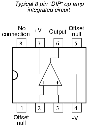
The following diagram shows the pin connections for single op-amps (741 included) when housed in an 8-pin DIP (Dual Inline Package) integrated circuit:
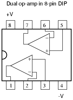
Some models of op-amp come two to a package, including the popular models TL082 and 1458. These are called 'dual' units, and are typically housed in an 8-pin DIP package as well, with the following pin connections:
Operational amplifiers are also available four to a package, usually in 14-pin DIP packages. Unfortunately, pin assignments aren't as standard for these 'quad' op-amps as they are for the 'dual' or single units. See the manufacturer datasheet for details.
Practical operational amplifier voltage gains are in the range of 200,000 or more, which makes them almost useless as an analog differential amplifier by themselves. For an op-amp with a voltage gain (AV) of 200,000 and a maximum output voltage swing of +15V/-15V, all it would take is a differential input voltage of 75 V (microvolts) to drive it to saturation or cutoff!
Application 1: the comparator
For all practical purposes, we can say that the output of an op-amp will be saturated fully positive if the (+) input is more positive than the (-) input, and saturated fully negative if the (+) input is less positive than the (-) input. In other words, an op-amp's extremely high voltage gain makes it useful as a device to compare two voltages and change output voltage states when one input exceeds the other in magnitude.
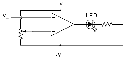
In the above circuit, we have an op-amp connected as a comparator, comparing the input voltage with a reference voltage set by the potentiometer (R1). If Vin drops below the voltage set by R1, the op-amp's output will saturate to +V, thereby lighting up the LED. Otherwise, if Vin is above the reference voltage, the LED will remain off. If Vin is a voltage signal produced by a measuring instrument, this comparator circuit could function as a 'low' alarm, with the trip-point set by R1. Instead of an LED, the op-amp output could drive a relay, a transistor, a thyristor, or any other device capable of switching power to a load.
Application 2: the comparator working as a square-wave converter.
Suppose that the input voltage applied to the inverting (-) input was an AC sine wave rather than a stable DC voltage. In that case, the output voltage would transition between opposing states of saturation whenever the input voltage was equal to the reference voltage produced by the potentiometer. The result would be a square wave:
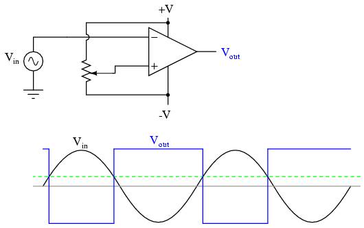
Adjustments to the potentiometer setting would change the reference voltage applied to the noninverting (+) input, which would change the points at which the sine wave would cross, changing the on/off times, or duty cycle of the square wave:
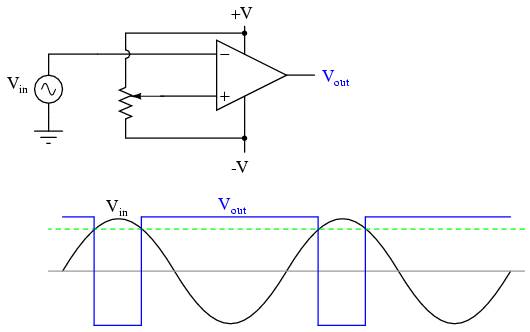
It should be evident that the AC input voltage would not have to be a sine wave in particular for this circuit to perform the same function. The input voltage could be a triangle wave, sawtooth wave, or any other sort of wave that ramped smoothly from positive to negative to positive again. This sort of comparator circuit is very useful for creating square waves of varying duty cycle. This technique is sometimes referred to as pulse-width modulation, or PWM (varying, or modulating, a waveform according to a controlling signal, in this case the signal produced by the potentiometer).
Another comparator application is that of the bargraph driver. If we had several op-amps connected as comparators, each with its own reference voltage connected to the inverting input, but each one monitoring the same voltage signal on their noninverting inputs, we could build a bargraph-style meter such as what is commonly seen on the face of stereo tuners and graphic equalizers. As the signal voltage (representing radio signal strength or audio sound level) increased, each comparator would 'turn on' in sequence and send power to its respective LED. With each comparator switching 'on' at a different level of audio sound, the number of LED's illuminated would indicate how strong the signal was.
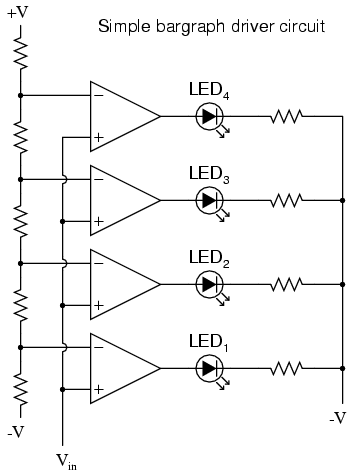
In the circuit shown above, LED1 would be the first to light up as the input voltage increased in a positive direction. As the input voltage continued to increase, the other LED's would illuminate in succession, until all were lit.
CONCLUSIONS:
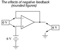
If we connect the output of an op-amp to its inverting input and apply a voltage signal to the noninverting input, we find that the output voltage of the op-amp closely follows that input voltage (It was neglected to draw in the power supply, +V/-V wires, and ground symbol for simplicity):
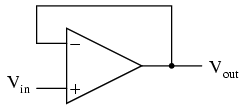
As Vin increases, Vout will increase in accordance with the differential gain. However, as Vout increases, that output voltage is fed back to the inverting input, thereby acting to decrease the voltage differential between inputs, which acts to bring the output down. What will happen for any given voltage input is that the op-amp will output a voltage very nearly equal to Vin, but just low enough so that there's enough voltage difference left between Vin and the (-) input to be amplified to generate the output voltage.
The circuit will quickly reach a point of stability (known as equilibrium in physics), where the output voltage is just the right amount to maintain the right amount of differential, which in turn produces the right amount of output voltage. Taking the op-amp's output voltage and coupling it to the inverting input is a technique known as negative feedback, and it is the key to having a self-stabilizing system (this is true not only of op-amps, but of any dynamic system in general). This stability gives the op-amp the capacity to work in its linear (active) mode, as opposed to merely being saturated fully 'on' or 'off' as it was when used as a comparator, with no feedback at all.
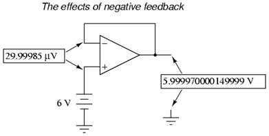
Because the op-amp's gain is so high, the voltage on the inverting input can be maintained almost equal to Vin. Let's say that our op-amp has a differential voltage gain of 200,000. If Vin equals 6 volts, the output voltage will be 5.999970000149999 volts. This creates just enough differential voltage (6 volts - 5.999970000149999 volts = 29.99985 V) to cause 5.999970000149999 volts to be manifested at the output terminal, and the system holds there in balance. As you can see, 29.99985 V is not a large value, so for practical calculations, we can assume that the differential voltage between the two input wires is held by negative feedback exactly at 0 volts.
One big advantage to using an op-amp with negative feedback is that the actual voltage gain of the op-amp doesn't matter, so long as it's very large. If the op-amp's differential gain were 250,000 instead of 200,000, all it would mean is that the output voltage would hold just a little closer to Vin (less differential voltage needed between inputs to generate the required output). In the circuit just illustrated, the output voltage would still be (for all practical purposes) equal to the non-inverting input voltage. Op-amp gains do not have to be precisely set by the factory in order for the circuit designer to build an amplifier circuit with precise gain. Negative feedback makes the system self-correcting. The above circuit as a whole will simply follow the input voltage with a stable gain of 1.
It should be mentioned that many op-amps cannot swing their output voltages exactly to +V/-V power supply rail voltages. The model 741 is one of those that cannot: when saturated, its output voltage peaks within about one volt of the +V power supply voltage and within about 2 volts of the -V power supply voltage. Therefore, with a split power supply of +15/-15 volts, a 741 op-amp's output may go as high as +14 volts or as low as -13 volts (approximately), but no further. This is due to its bipolar transistor design. These two voltage limits are known as the positive saturation voltage and negative saturation voltage, respectively. Other op-amps, such as the model 3130 with field-effect transistors in the final output stage, have the ability to swing their output voltages within millivolts of either power supply rail voltage. Consequently, their positive and negative saturation voltages are practically equal to the supply voltages.
CONCLUSIONS:
If we add a voltage divider to the negative feedback wiring so that only a fraction of the output voltage is fed back to the inverting input instead of the full amount, the output voltage will be a multiple of the input voltage:
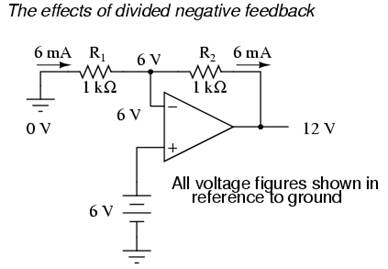
If R1 and R2 are both equal and Vin is 6 volts, the op-amp will output whatever voltage is needed to drop 6 volts across R1 (to make the inverting input voltage equal to 6 volts, as well, keeping the voltage difference between the two inputs equal to zero). With the 2:1 voltage divider of R1 and R2, this will take 12 volts at the output of the op-amp to accomplish.
Another way of analyzing this circuit is to start by calculating the magnitude and direction of current through R1, knowing the voltage on either side (and therefore, by subtraction, the voltage across R1), and R1's resistance. Since the left-hand side of R1 is connected to ground (0 volts) and the right-hand side is at a potential of 6 volts (due to the negative feedback holding that point equal to Vin), we can see that we have 6 volts across R1. This gives us 6 mA of current through R1 from left to right. Because we know that both inputs of the op-amp have extremely high impedance, we can safely assume they won't add or subtract any current through the divider. In other words, we can treat R1 and R2 as being in series with each other: all of the electrons flowing through R1 must flow through R2. Knowing the current through R2 and the resistance of R2, we can calculate the voltage across R2 (6 volts), and its polarity. Counting up voltages from ground (0 volts) to the right-hand side of R2, we arrive at 12 volts on the output.
We can change the voltage gain of this circuit, overall, just by adjusting the values of R1 and R2 (changing the ratio of output voltage that is fed back to the inverting input).
Gain can be calculated by the following formula:
![]()
Note that the voltage gain for this design of amplifier circuit can never be less than 1. If we were to lower R2 to a value of zero ohms, our circuit would be essentially identical to the voltage follower, with the output directly connected to the inverting input. Since the voltage follower has a gain of 1, this sets the lower gain limit of the noninverting amplifier. However, the gain can be increased far beyond 1, by increasing R2 in proportion to R1.
Also note that the polarity of the output matches that of the input, just as with a voltage follower. A positive input voltage results in a positive output voltage, and vice versa (with respect to ground). For this reason, this circuit is referred to as a noninverting amplifier.
Just as with the voltage follower, we see that the differential gain of the op-amp is irrelevant, so long as it's very high. The voltages and currents in this circuit would hardly change at all if the op-amp's voltage gain were 250,000 instead of 200,000. This stands as a stark contrast to single-transistor amplifier circuit designs, where the Beta of the individual transistor greatly influenced the overall gains of the amplifier. With negative feedback, we have a self-correcting system that amplifies voltage according to the ratios set by the feedback resistors, not the gains internal to the op-amp.
Let's see what happens if we retain negative feedback through a voltage divider, but apply the input voltage at a different location:
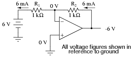
By grounding the noninverting input, the negative feedback from the output seeks to hold the inverting input's voltage at 0 volts, as well. For this reason, the inverting input is referred to in this circuit as a virtual ground, being held at ground potential (0 volts) by the feedback, yet not directly connected to (electrically common with) ground. The input voltage this time is applied to the left-hand end of the voltage divider (R1 = R2 = 1 kΩ again), so the output voltage must swing to -6 volts in order to balance the middle at ground potential (0 volts). Using the same techniques as with the noninverting amplifier, we can analyze this circuit's operation by determining current magnitudes and directions, starting with R1, and continuing on to determining the output voltage.
We can change the overall voltage gain of this circuit, overall, just by adjusting the values of R1 and R2 (changing the ratio of output voltage that is fed back to the inverting input).
Gain can be calculated by the following formula:
![]()
Note that this circuit's voltage gain can be less than 1, depending solely on the ratio of R2 to R1. Also note that the output voltage is always the opposite polarity of the input voltage. A positive input voltage results in a negative output voltage, and vice versa (with respect to ground). For this reason, this circuit is referred to as an inverting amplifier. Sometimes, the gain formula contains a negative sign (before the R2/R1 fraction) to reflect this reversal of polarities.
These two amplifier circuits we've just investigated serve the purpose of multiplying or dividing the magnitude of the input voltage signal. This is exactly how the mathematical operations of multiplication and division are typically handled in analog computer circuitry.
CONCLUSIONS:
If three equal resistors are taken and connected one end of each to a common point, then apply three input voltages (one to each of the resistors' free ends), the voltage seen at the common point will be the mathematical average of the three.
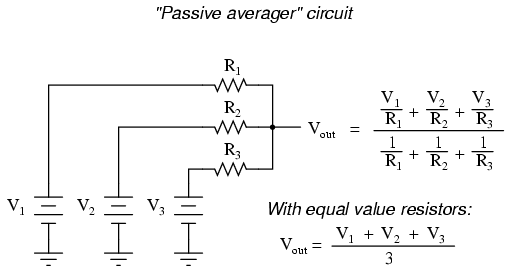
This circuit is really nothing more than a practical application of Millman's Theorem:
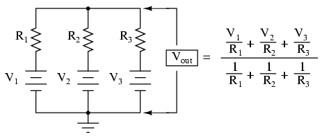
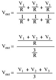
This circuit is commonly known as a passive averager, because it generates an average voltage with non-amplifying components. Passive simply means that it is an unamplified circuit. The large equation to the right of the averager circuit comes from Millman's Theorem, which describes the voltage produced by multiple voltage sources connected together through individual resistances. Since the three resistors in the averager circuit are equal to each other, we can simplify Millman's formula by writing R1, R2, and R3 simply as R (one, equal resistance instead of three individual resistances):
If we take a passive averager and use it to connect three input voltages into an op-amp amplifier circuit with a gain of 3, we can turn this averaging function into an addition function. The result is called a noninverting summer circuit:
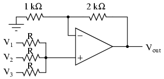
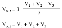
With a voltage divider composed of a 2 kΩ / 1 kΩ combination, the noninverting amplifier circuit will have a voltage gain of 3. By taking the voltage from the passive averager, which is the sum of V1, V2, and V3 divided by 3, and multiplying that average by 3, we arrive at an output voltage equal to the sum of V1, V2, and V3:
Much the same can be done with an inverting op-amp amplifier, using a passive averager as part of the voltage divider feedback circuit. The result is called an inverting summer circuit:
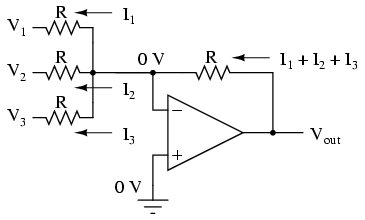
Now, with the right-hand sides of the three averaging resistors connected to the virtual ground point of the op-amp's inverting input, Millman's Theorem no longer directly applies as it did before. The voltage at the virtual ground is now held at 0 volts by the op-amp's negative feedback, whereas before it was free to float to the average value of V1, V2, and V3. However, with all resistor values equal to each other, the currents through each of the three resistors will be proportional to their respective input voltages. Since those three currents will add at the virtual ground node, the algebraic sum of those currents through the feedback resistor will produce a voltage at Vout equal to V1 + V2 + V3, except with reversed polarity. The reversal in polarity is what makes this circuit an inverting summer:
![]()
Summer (adder) circuits are quite useful in analog computer design, just as multiplier and divider circuits would be. Again, it is the extremely high differential gain of the op-amp which allows us to build these useful circuits with a bare minimum of components.
CONCLUSIONS:
By introducing electrical reactance into the feedback loops of op-amp amplifier circuits, we can cause the output to respond to changes in the input voltage over time. Drawing their names from their respective calculus functions, the integrator produces a voltage output proportional to the product (multiplication) of the input voltage and time; and the differentiator (not to be confused with differential) produces a voltage output proportional to the input voltage's rate of change.
Capacitance can be defined as the measure of a capacitor's opposition to changes in voltage. The greater the capacitance, the more the opposition. Capacitors oppose voltage change by creating current in the circuit: that is, they either charge or discharge in response to a change in applied voltage. So, the more capacitance a capacitor has, the greater its charge or discharge current will be for any given rate of voltage change across it. The equation for this is quite simple:
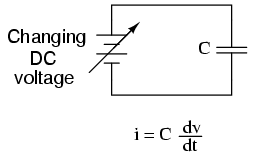
The dv/dt fraction is a calculus expression representing the rate of voltage change over time. If the DC supply in the above circuit were steadily increased from a voltage of 15 volts to a voltage of 16 volts over a time span of 1 hour, the current through the capacitor would most likely be very small, because of the very low rate of voltage change (dv/dt = 1 volt / 3600 seconds). However, if we steadily increased the DC supply from 15 volts to 16 volts over a shorter time span of 1 second, the rate of voltage change would be much higher, and thus the charging current would be much higher (3600 times higher, to be exact). Same amount of change in voltage, but vastly different rates of change, resulting in vastly different amounts of current in the circuit.
To put some definite numbers to this formula, if the voltage across a 47 F capacitor was changing at a linear rate of 3 volts per second, the current 'through' the capacitor would be (47 F)(3 V/s) = 141 A.
We can build an op-amp circuit which measures change in voltage by measuring current through a capacitor, and outputs a voltage proportional to that current:
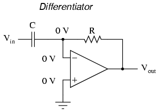
The right-hand side of the capacitor is held to a voltage of 0 volts, due to the 'virtual ground' effect. Therefore, current 'through' the capacitor is solely due to change in the input voltage. A steady input voltage won't cause a current through C, but a changing input voltage will.
Capacitor current moves through the feedback resistor, producing a drop across it, which is the same as the output voltage. A linear, positive rate of input voltage change will result in a steady negative voltage at the output of the op-amp. Conversely, a linear, negative rate of input voltage change will result in a steady positive voltage at the output of the op-amp. This polarity inversion from input to output is due to the fact that the input signal is being sent (essentially) to the inverting input of the op-amp, so it acts like the inverting amplifier mentioned previously. The faster the rate of voltage change at the input (either positive or negative), the greater the voltage at the output.
The formula for determining voltage output for the differentiator is as follows:
![]()
Applications for this, besides representing the derivative calculus function inside of an analog computer, include rate-of-change indicators for process instrumentation. The DC voltage produced by the differentiator circuit could be used to drive a comparator, which would signal an alarm or activate a control if the rate of change exceeded a pre-set level.
In process control, the derivative function is used to make control decisions for maintaining a process at setpoint, by monitoring the rate of process change over time and taking action to prevent excessive rates of change, which can lead to an unstable condition. Analog electronic controllers use variations of this circuitry to perform the derivative function.
On the other hand, there are applications where we need precisely the opposite function, called integration in calculus. Here, the op-amp circuit would generate an output voltage proportional to the magnitude and duration that an input voltage signal has deviated from 0 volts. Stated differently, a constant input signal would generate a certain rate of change in the output voltage: differentiation in reverse. To do this, all we have to do is swap the capacitor and resistor in the previous circuit:
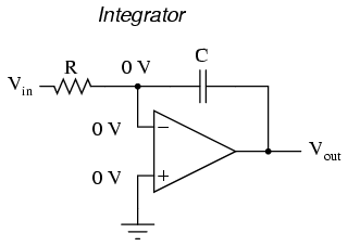
As before, the negative feedback of the op-amp ensures that the inverting input will be held at 0 volts (the virtual ground). If the input voltage is exactly 0 volts, there will be no current through the resistor, therefore no charging of the capacitor, and therefore the output voltage will not change. We cannot guarantee what voltage will be at the output with respect to ground in this condition, but we can say that the output voltage will be constant.
However, if we apply a constant, positive voltage to the input, the op-amp output will fall negative at a linear rate, in an attempt to produce the changing voltage across the capacitor necessary to maintain the current established by the voltage difference across the resistor. Conversely, a constant, negative voltage at the input results in a linear, rising (positive) voltage at the output. The output voltage rate-of-change will be proportional to the value of the input voltage.
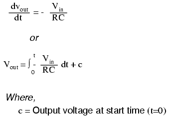
The formula for determining voltage output for the integrator is as follows:
One application: to keep a 'running total' of radiation exposure, or dosage, if the input voltage was a proportional signal supplied by an electronic radiation detector. Nuclear radiation can be just as damaging at low intensities for long periods of time as it is at high intensities for short periods of time. An integrator circuit would take both the intensity (input voltage magnitude) and time into account, generating an output voltage representing total radiation dosage.
Another application: to integrate a signal representing water flow, producing a signal representing total quantity of water that has passed by the flowmeter. This application of an integrator is sometimes called a totalizer in the industrial instrumentation trade.
CONCLUSIONS:
The negative feedback is an incredibly useful principle when applied to operational amplifiers. It is what allows us to create all these practical circuits, being able to precisely set gains, rates, and other significant parameters with just a few changes of resistor values. Negative feedback makes all these circuits stable and self-correcting.
The basic principle of negative feedback is that the output tends to drive in a direction that creates a condition of equilibrium (balance). In an op-amp circuit with no feedback, there is no corrective mechanism, and the output voltage will saturate with the tiniest amount of differential voltage applied between the inputs. The result is a comparator.
Another type of feedback, namely positive feedback, also finds application in op-amp circuits. Unlike negative feedback, where the output voltage is 'fed back' to the inverting (-) input, with positive feedback the output voltage is somehow routed back to the noninverting (+) input. In its simplest form, we could connect a straight piece of wire from output to noninverting input and see what happens:
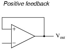
The inverting input remains disconnected from the feedback loop, and is free to receive an external voltage. Let's see what happens if we ground the inverting input:
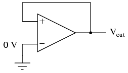
With the inverting input grounded (maintained at zero volts), the output voltage will be dictated by the magnitude and polarity of the voltage at the noninverting input. If that voltage happens to be positive, the op-amp will drive its output positive as well, feeding that positive voltage back to the noninverting input, which will result in full positive output saturation. On the other hand, if the voltage on the noninverting input happens to start out negative, the op-amp's output will drive in the negative direction, feeding back to the noninverting input and resulting in full negative saturation.
What we have here is a circuit whose output is bistable: stable in one of two states (saturated positive or saturated negative). Once it has reached one of those saturated states, it will tend to remain in that state, unchanging. What is necessary to get it to switch states is a voltage placed upon the inverting (-) input of the same polarity, but of a slightly greater magnitude. For example, if our circuit is saturated at an output voltage of +12 volts, it will take an input voltage at the inverting input of at least +12 volts to get the output to change. When it changes, it will saturate fully negative.
So, an op-amp with positive feedback tends to stay in whatever output state it's already in. It 'latches' between one of two states, saturated positive or saturated negative. Technically, this is known as hysteresis.
An important application of positive feedback in the case of the op-amp circuits is the oscillator circuit (shortly named oscillator). An oscillator is a device that produces an alternating (AC), or at least pulsing, output voltage. Technically, it is known as an astable device: having no stable output state (no equilibrium whatsoever). Oscillators are very useful devices, and they are easily made with just an op-amp and a few external components.
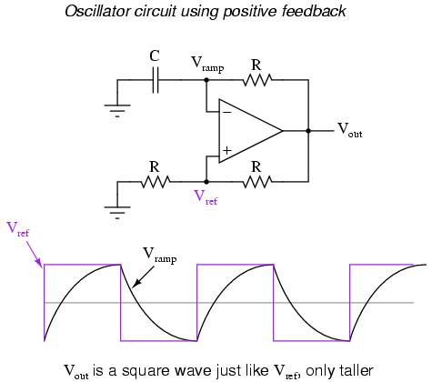
When the output is saturated positive, the Vref will be positive, and the capacitor will charge up in a positive direction. When Vramp exceeds Vref by the tiniest margin, the output will saturate negative, and the capacitor will charge in the opposite direction (polarity). Oscillation occurs because the positive feedback is instantaneous and the negative feedback is delayed (by means of an RC time constant). The frequency of this oscillator may be adjusted by varying the size of any component.
CONCLUSIONS:
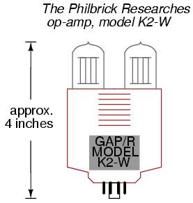
1. Operational amplifier using vacuum electronic tubes
While mention of operational amplifiers typically provokes visions of semiconductor devices built as integrated circuits on a miniature silicon chip, the first op-amps were actually vacuum tube circuits. The first commercial, general purpose operational amplifier was manufactured by the George A. Philbrick Researches, Incorporated, in 1952. Designated the K2-W, it was built around two twin-triode tubes mounted in an assembly with an octal (8-pin) socket for easy installation and servicing in electronic equipment chassis of that era. The assembly looked something like this:
The schematic diagram shows the two tubes, along with ten resistors and two capacitors, a fairly simple circuit design even by 1952 standards:
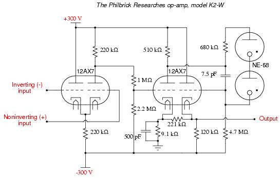
With a dual-supply voltage of +300/-300 volts, this op-amp could only swing its output +/- 50 volts, which is very poor by today's standards. It had an open-loop voltage gain of 15,000 to 20,000, a slew rate of +/- 12 volts/second, a maximum output current of 1 mA, a quiescent power consumption of over 3 watts (not including power for the tubes' filaments!).
2. Operational amplifier using discrete solid-state transistors
With the advent of solid-state transistors, op-amps with far less quiescent power consumption and increased reliability became feasible, but many of the other performance parameters remained about the same. Take for instance Philbrick's model P55A, a general-purpose solid-state op-amp circa 1966. The P55A sported an open-loop gain of 40,000, a slew rate of 1.5 volt/second and an output swing of +/- 11 volts (at a power supply voltage of +/- 15 volts), a maximum output current of 2.2 mA. The P55A, as well as other op-amps in Philbrick's lineup of the time, was of discrete-component construction, its constituent transistors, resistors, and capacitors housed in a solid 'brick' resembling a large integrated circuit package.
A schematic of one such circuit is shown here:
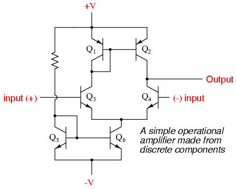
While its performance is rather dismal by modern standards, it demonstrates that complexity is not necessary to create a minimally functional op-amp. Transistors Q3 and Q4 form the heart of another differential pair circuit, the semiconductor equivalent of the first triode tube in the K2-W schematic. As it was in the vacuum tube circuit, the purpose of a differential pair is to amplify and convert a differential voltage between the two input terminals to a single-ended output voltage.
2. Operational amplifier using integrated-circuit (IC) technology
With the advent of integrated-circuit (IC) technology, op-amp designs experienced a dramatic increase in performance, reliability, density, and economy. Between the years of 1964 and 1968, the Fairchild corporation introduced three models of IC op-amps: the 702, 709, and the still-popular 741. While the 741 is now considered outdated in terms of performance, it is still a favorite among hobbyists for its simplicity and fault tolerance (short-circuit protection on the output, for instance)..
The internal schematic diagram for a model 741 op-amp is as follows:
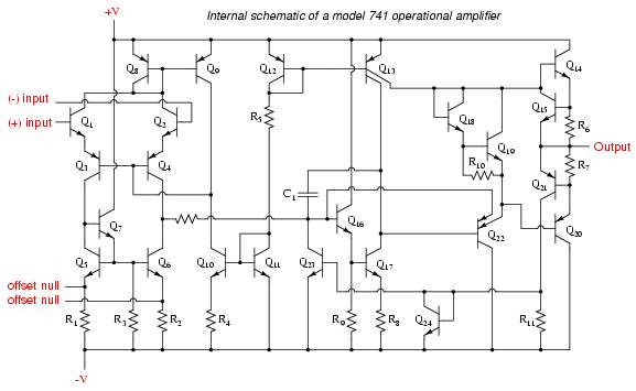
By integrated circuit standards, the 741 is a very simple device: an example of small-scale integration, or SSI technology. It would be no small matter to build this circuit using discrete components, so you can see the advantages of even the most primitive integrated circuit technology over discrete components where high parts counts are involved.
For the practical design and work, there are hundreds of op-amp models to choose from. Special-purpose instrumentation and radio-frequency (RF) op-amps may be quite a bit more expensive. The 741 is included as a 'benchmark' for comparison, although it is considered today an obsolete design.
Widely used operational amplifiers
|
Model |
Devices/ package |
Power supply |
Bandwidth |
Bias current |
Slew rate |
Output current |
|
number |
(count) |
(V) |
(Mhz) |
(nA) |
(V/S) |
(mA) |
|
TL082 | ||||||
|
LM301A | ||||||
|
LM318 | ||||||
|
LM324 | ||||||
|
LF353 | ||||||
|
LF356 | ||||||
|
LF411 | ||||||
|
741C | ||||||
|
LM833 | ||||||
|
LM1458 | ||||||
|
CA3130 |
Take for instance the parameter of input bias current: the CA3130 wins the prize for lowest, at 0.05 nA (or 50 pA), and the LM833 has the highest at slightly over 1 A. The model CA3130 achieves its incredibly low bias current through the use of MOSFET transistors in its input stage. One manufacturer advertises the 3130's input impedance as 1.5 tera-ohms, or 1.5 x 10¹² Ω! Other op-amps shown here with low bias current figures use JFET input transistors, while the high bias current models use bipolar input transistors.
While the 741 is specified in many electronic project schematics and showcased in many textbooks, its performance has long been surpassed by other designs in every measure. Even some designs originally based on the 741 have been improved over the years to far surpass original design specifications. One such example is the model 1458, two op-amps in an 8-pin DIP package, which at one time had the exact same performance specifications as the single 741. In its latest incarnation it boasts a wider power supply voltage range, a slew rate 50 times as great, and almost twice the output current capability of a 741, while still retaining the output short-circuit protection feature of the 741. Op-amps with JFET and MOSFET input transistors far exceed the 741's performance in terms of bias current, and generally manage to beat the 741 in terms of bandwidth and slew rate as well.
Recommendations for op-amps:
When low bias current is a priority (such as in low-speed integrator circuits), choose the
For general-purpose DC amplifier work, the offers good performance (and you get two op-amps in the space of one package). For an upgrade in performance, choose the model , as it is a pin-compatible replacement for the 1458.
The 353 is designed with JFET input circuitry for very low bias current, and has a bandwidth 4 times are great as the 1458, although its output current limit is lower (but still short-circuit protected). It may be more difficult to find on the shelf of your local electronics supply house, but it is just as reasonably priced as the 1458.
If low power supply voltage is a requirement, it is recommended the model , as it functions on as low as 3 volts DC. Its input bias current requirements are also low, and it provides four op-amps in a single 14-pin chip. Its major weakness is speed, limited to 1 MHz bandwidth and an output slew rate of only 0.25 volts per s.
For high-frequency AC amplifier circuits, the is a very good 'general purpose' model.
Special-purpose op-amps are available for modest cost which provide better performance specifications. Many of these are tailored for a specific type of performance advantage, such as maximum bandwidth or minimum bias current. Take for instance the op-amps, both designed for high bandwidth in table below
High bandwidth operational amplifiers
|
Model |
Devices/ package |
Power supply |
Bandwidth |
Bias current |
Slew rate |
Output current |
|
number |
(count) |
(V) |
(Mhz) |
(nA) |
(V/S) |
(mA) |
|
CLC404 | ||||||
|
CLC425 |
Some op-amps, designed for high power output are listed in the following table.
High current operational amplifiers
|
Model |
Devices/ package |
Power supply |
Bandwidth |
Bias current |
Slew rate |
Output current |
|
number |
(count) |
(V) |
(Mhz) |
(nA) |
(V/S) |
(mA) |
|
LM12CL | ||||||
|
LM7171 |
LM12CL actually has an output current rating of 13 amps (13,000 milliamps)! The LM7171, on the other hand, trades high current output ability for fast voltage output ability (a high slew rate).
Amplifier packages may also be purchased as complete application circuits as opposed to bare operational amplifiers. The Burr-Brown and Analog Devices corporations, for example, both long known for their precision amplifier product lines, offer instrumentation amplifiers in pre-designed packages as well as other specialized amplifier devices. In designs where high precision and repeatability after repair is important, it might be advantageous for the circuit designer to choose such a pre-engineered amplifier 'block' rather than build the circuit from individual op-amps.
|
Politica de confidentialitate | Termeni si conditii de utilizare |

Vizualizari: 2377
Importanta: ![]()
Termeni si conditii de utilizare | Contact
© SCRIGROUP 2025 . All rights reserved